
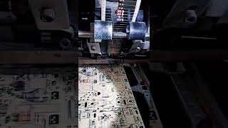
Case Study 2: Copper Barrier Layer Delamination in BEOL
Interactive Audio Lesson
Listen to a student-teacher conversation explaining the topic in a relatable way.
Delamination Issues in BEOL
🔒 Unlock Audio Lesson
Sign up and enroll to listen to this audio lesson

Today, we're going to discuss the delamination issue we faced in the copper barrier layer during 7nm interconnect fabrication. Can anyone tell me what delamination means?

Isn't it when layers separate from each other?
Exactly! Delamination refers to the separation of layers that can lead to failures like voids in copper vias. Let's dive into what caused this in our case study.

What were the main reasons for this delamination?
Great question! The root causes we identified included surface roughness and plasma damage during the etch-back step. These factors compromised the adhesion of the barrier layer.

How does surface roughness affect adhesion?
The rougher the surface, the more difficult it becomes for materials to bond effectively. Think of it like trying to glue together two uneven pieces; it's much harder than gluing flat surfaces.

What exactly is the ALD liner?
The ALD liner is a layer deposited using atomic layer deposition, crucial for creating a conformal barrier. Improper densification was another factor that negatively impacted adhesion.
In summary, we identified delamination in the copper barrier layer due to poor adhesion caused by surface roughness and plasma damage. Any questions before we move on?
Identifying Solutions
🔒 Unlock Audio Lesson
Sign up and enroll to listen to this audio lesson

Now, let's consider the solutions we implemented to address the delamination issues. Can anyone suggest what actions could improve layer adhesion?
Using a different material for the barrier could help!
That's a solid idea! In our case, we replaced the PVD barrier with a conformal ALD barrier, which significantly improved adhesion.
What else did you do?
We also introduced a plasma pre-clean before liner deposition to prepare the surface for better adhesion. This method effectively removes any contaminants.
Did you gauge the success of these modifications?
Yes! We implemented in-line acoustic inspection to continuously monitor the integrity of our vias. This helped ensure our adjustments were effective.
What was the outcome of these interventions?
Well, we observed an impressive fivefold improvement in via reliability and reduced voids down to less than 0.5%. It was a significant success!
To summarize, we addressed the delamination by changing materials and modifying our cleaning processes, resulting in excellent improvements in product quality.
Root Cause Analysis
🔒 Unlock Audio Lesson
Sign up and enroll to listen to this audio lesson
Now, let's discuss root cause analysis or RCA. Why do you think it's critical in solving engineering problems?
To find the underlying issues so we don't just treat the symptoms?
Exactly! In our case study, performing RCA revealed the critical factors leading to delamination. What was one of the main issues we found?
Surface roughness and plasma damage!
Right! Recognizing these root causes allowed us to implement targeted solutions rather than general fixes. This is a key principle in engineering.
How do you typically carry out a root cause analysis?
We generally collaborate with a team to gather data, identify failure patterns, and use tools like Fishbone diagrams or the 5 Whys technique to drill down to the real causes.
In summary, RCA is essential because it helps us pinpoint and solve the true issues rather than merely addressing symptoms. Any final thoughts on this topic?
Introduction & Overview
Read summaries of the section's main ideas at different levels of detail.
Quick Overview
Standard
The copper barrier layer delamination case study details the problems encountered in 7nm interconnect fabrication due to poor adhesion of the TaN barrier layer. It identifies root causes, including surface imperfections and processing errors, and discusses effective engineering modifications that resulted in a significant improvement in via reliability.
Detailed
Detailed Summary
In this section, the focus is on a specific issue encountered during the 7nm interconnect fabrication process related to copper vias. Engineers discovered that delamination and voids formed in the copper vias when subjected to reliability testing.
Key Points Discussed:
- Background: The challenge emerged during the reliability testing phase, where voids and delamination were prominent.
- Problem Identified: The main issue was linked to the TaN barrier layer, which failed to adhere properly to the dielectric material during the physical vapor deposition (PVD) process.
- Root Cause Analysis (RCA): Two significant factors contributed to the failure:
- Surface Roughness: The dielectric had surface roughness that undermined the adhesive quality during the barrier layer application.
- Plasma Damage: Damage inflicted during etch-back steps further degraded the adhesion properties.
- Improper Densification of ALD liner: An inadequately densified atomic layer deposition (ALD) liner exacerbated the adhesion issues.
- Engineering Solutions: To rectify the situation, several interventions were made:
- A plasma pre-clean was introduced before the deposition of the liner to enhance bonding.
- The PVD barrier layer was replaced with a conformal ALD barrier (specifically a TaN + Ru stack) for improved performance.
- An in-line acoustic inspection method was deployed to monitor defects.
- Outcome: These changes resulted in a fivefold increase in the reliability of the vias and a reduction in the occurrence of voids to less than 0.5% of the cross-sections.
This case study highlights the importance of addressing integration issues in semiconductor fabrication, showing how targeted adjustments can lead to significantly enhanced outcomes.
Youtube Videos


Audio Book
Dive deep into the subject with an immersive audiobook experience.
Background of the Case Study
Chapter 1 of 5
🔒 Unlock Audio Chapter
Sign up and enroll to access the full audio experience
Chapter Content
In 7nm interconnect fabrication, engineers found voids and delamination in copper vias during reliability testing.
Detailed Explanation
In semiconductor manufacturing, especially at advanced technology nodes like 7nm, the integrity of interconnects (the pathways that connect different parts of a chip) is critical for performance. This background indicates that during testing, which evaluates how well the copper vias (short vertical connections between different layers) held up under stress, issues were discovered. Voids (tiny gaps) and delamination (the process where layers of materials separate) can lead to failures in electrical connections, jeopardizing the functionality of the chip.
Examples & Analogies
Think of the copper vias like a highway connection between cities. If the road (via) has potholes (voids) or if parts of the road surface start peeling away (delamination), cars (electric signals) can't travel smoothly, leading to traffic jams (functional failures) and making travel inefficient.
Identifying the Problem
Chapter 2 of 5
🔒 Unlock Audio Chapter
Sign up and enroll to access the full audio experience
Chapter Content
The TaN barrier layer did not adhere well to the underlying dielectric during PVD.
Detailed Explanation
The problem identified was related to the adhesion of the titanium nitride (TaN) barrier layer over the dielectric material during the Physical Vapor Deposition (PVD) process. The barrier layer is crucial because it prevents copper from diffusing into the dielectric, which can cause reliability issues. Poor adhesion means that the barrier might fail, leading to issues like delamination that were observed during testing.
Examples & Analogies
Imagine applying a new coat of paint (TaN layer) over a wall (dielectric material). If the wall is dirty or uneven, the paint won’t stick well. As a result, it may peel off, just like the barrier layer isn’t sticking properly to the dielectric, eventually leading to failures.
Root Cause Analysis
Chapter 3 of 5
🔒 Unlock Audio Chapter
Sign up and enroll to access the full audio experience
Chapter Content
Surface roughness and plasma damage during etch-back step degraded adhesion. ALD liner was improperly densified.
Detailed Explanation
Root cause analysis revealed two main factors that contributed to the delamination. First, the surface roughness of the dielectric affected how well the barrier layer could stick. Second, during a specific step known as etch-back, plasma damage occurred which further compromised the adhesion. Additionally, the Atomic Layer Deposition (ALD) liner was not properly densified, meaning it didn't form a solid enough layer to support the subsequent barrier deposition.
Examples & Analogies
It's like trying to glue two pieces of wood together. If one piece is rough and not sanded properly (surface roughness) or if you accidentally burn the edges with a flame (plasma damage), the glue (TaN) won’t hold effectively, leading to separation.
Solutions Implemented
Chapter 4 of 5
🔒 Unlock Audio Chapter
Sign up and enroll to access the full audio experience
Chapter Content
Added plasma pre-clean before liner deposition. Replaced PVD barrier with conformal ALD barrier (TaN + Ru stack). Introduced in-line acoustic inspection.
Detailed Explanation
Several solutions were implemented to address the delamination issue. A plasma pre-clean step was added before depositing the liner to ensure a clean, well-prepared surface that would allow for better adhesion. The PVD barrier was replaced with a conformal ALD barrier, which allows for a more uniform coating over complex surfaces. Additionally, in-line acoustic inspection technology was introduced to monitor the integrity of the vias and detect any issues early in the process.
Examples & Analogies
Think of it like preparing a surface for painting. You might clean it and sand it down (plasma pre-clean) to ensure the paint sticks well. Instead of using a paint that only covers the top of an uneven surface (PVD), you use a spray that gets into every crack and crevice (ALD), ensuring full coverage. Lastly, periodically checking the paint application for defects (acoustic inspection) ensures any problems are caught before they become serious.
Outcome of the Solutions
Chapter 5 of 5
🔒 Unlock Audio Chapter
Sign up and enroll to access the full audio experience
Chapter Content
Via reliability improved by 5×, and voids were reduced to <0.5% of cross-sections.
Detailed Explanation
The implementation of these solutions led to a significant improvement in reliability – the vias became five times more reliable, meaning they were much less likely to fail under stress. Furthermore, the occurrence of voids was dramatically reduced, indicating that the measures taken effectively addressed the problems observed in the original testing.
Examples & Analogies
Returning to our highway analogy, after paving the road properly and using better materials, traffic now flows smoothly without the previous potholes or rough patches (voids), ensuring that travel (electrical signals) is safe and efficient.
Key Concepts
-
Delamination: The separation of layers in materials leading to defects.
-
Barrier Layer: A crucial layer that prevents material diffusion.
-
Surface Roughness: A relevant property affecting adhesion in semiconductor processes.
-
Root Cause Analysis (RCA): A systematic approach to identifying the root causes of problems.
Examples & Applications
In 7nm IC fabrication, issues arose with copper vias due to delamination of the barrier layer, impacting reliability.
The introduction of a plasma pre-clean helped significantly enhance the adhesion of barrier layers in semiconductor processes.
Memory Aids
Interactive tools to help you remember key concepts
Rhymes
Delamination's a big confundation, when layers break, it's a fabrication!
Stories
Once in a factory, layers danced together. But the rough surface made them part forever. They learned that a clean start, plasma and attention, kept their bond strong, avoiding separation!
Memory Tools
A simple way to remember adhesion issues: 'Rough, Plasma, Densify' - think of these three RPD factors together to ensure strong bonds.
Acronyms
RPA (Roughness, Plasma, ALD) - Keep this acronym in mind when addressing adhesion issues in semiconductor processing.
Flash Cards
Glossary
- Delamination
The separation of layers in a material, often resulting in defects.
- Barrier Layer
A layer that prevents interlayer diffusion in semiconductor devices.
- Surface Roughness
A measure of the texture of a surface, affecting adhesion properties.
- Atomic Layer Deposition (ALD)
A thin film deposition technique that deposits materials layer by layer.
- Physical Vapor Deposition (PVD)
A process of depositing thin films by vaporizing a solid source material.
- Plasma PreClean
A cleaning process that uses plasma to remove contaminants from surfaces.
- Inline Inspection
Continuous monitoring of processes and products during fabrication.
Reference links
Supplementary resources to enhance your learning experience.