
Discussion on Common Base and Common Gate Amplifiers
Enroll to start learning
You’ve not yet enrolled in this course. Please enroll for free to listen to audio lessons, classroom podcasts and take practice test.
Interactive Audio Lesson
Listen to a student-teacher conversation explaining the topic in a relatable way.
Motivation for Common Base and Common Gate Amplifiers
🔒 Unlock Audio Lesson
Sign up and enroll to listen to this audio lesson

Welcome, class! Today we're diving into the common base (CB) and common gate (CG) amplifiers. Can anyone tell me why these configurations might be useful in analog circuits?

I think they help prevent loading effects from degrading the signal.
Exactly right! The common base and common gate configurations are primarily utilized to mitigate loading effects by functioning as current mode buffers. This allows for improved gain and bandwidth. Can anyone summarize what the loading effect is?

The loading effect occurs when the output impedance of one stage interacts with the input of the following stage, potentially reducing overall gain.
Great summary! Remember, the motivation for using CB and CG amplifiers is to maintain circuit performance without compromising speed or gain. Let's move on to discuss their basic operations.
Basic Operation of Common Base and Common Gate Amplifiers
🔒 Unlock Audio Lesson
Sign up and enroll to listen to this audio lesson

Now, let’s delve into the basic operation of these two amplifier configurations. How does the common base amplifier function?

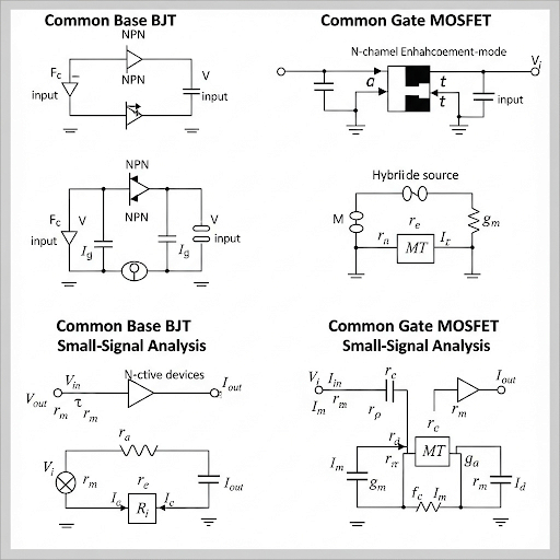
In a common base BJT amplifier, the input signal is applied to the emitter, while the output is taken from the collector.
Correct! The output signal at the collector is in phase with the input at the emitter, and they share a linear relationship. What about the common gate configuration?

For the common gate MOSFET amplifier, the input signal is applied to the source, and output is taken from the drain.
Absolutely right! Both configurations allow amplification of signals while preventing distortion. Remember, signals must not lead to cutoff states. Can someone explain in-phase operations for these amplifiers?
As the input rises, the collector or drain current decreases, which means the output voltage rises, maintaining the phase relationship.
Excellent! Understanding these basic operational principles is crucial for circuit design. Let’s now transition to biasing these amplifiers.
Biasing of Common Base and Common Gate Amplifiers
🔒 Unlock Audio Lesson
Sign up and enroll to listen to this audio lesson
Now that we’ve covered the operations, let's discuss biasing these configurations. Why is biasing critical in amplifiers?
Proper biasing ensures that the amplifier operates in its active region, allowing for linear amplification of input signals.
Exactly! For the common base amplifier, what biasing arrangements can we consider?
We could use a transistor-based biasing setup that matches the DC conditions to the input signal without disturbing the operating point.
Good point! A simple arrangement might involve using resistors or another transistor to set the DC levels. How about the common gate MOSFET configuration?
Similar to the common base, an active biasing scheme can stabilize the voltage levels at the gate and source.
Precisely! Biasing is crucial for reliable signal amplification by ensuring that devices operate efficiently. Now, let’s analyze their performance metrics.
Performance Analysis of Common Base and Common Gate Amplifiers
🔒 Unlock Audio Lesson
Sign up and enroll to listen to this audio lesson
Let’s dive into the performance metrics of CB and CG amplifiers such as voltage gain, input and output impedance. What can you tell me about the voltage gain?
The voltage gain in both configurations is generally greater than one and is often dependent on the load conditions.
Right on! The input impedance for the common base is low, but can someone explain the input impedance characteristics of the common gate?
The common gate amplifier has a low input impedance as well, but the output impedance is much higher compared to its input.
Exactly! And this is complementary to the common emitter and common drain configurations. What does that mean for practical applications?
It allows better matching of impedance between stages, reducing signal loss and ensuring effective amplification.
Correct! These key metrics – voltage gain, input and output impedance – guide us in designing efficient and effective amplifiers. Let’s summarize what we’ve discussed today.
Introduction & Overview
Read summaries of the section's main ideas at different levels of detail.
Quick Overview
Standard
This section delves into the characteristics and essential functions of common base amplifiers (BJT) and common gate amplifiers (MOSFET). It includes the motivation for their use in circuit design, basic operational principles, biasing methods, and analyses of key performance parameters such as voltage gain, input and output impedance.
Detailed
Discussion on Common Base and Common Gate Amplifiers
This section focuses on the analysis and applications of the common base (CB) and common gate (CG) amplifier configurations, which serve critical roles in analog circuits. The discussion begins with motivation for utilizing these configurations as current mode buffers in circuits where voltage mode performance is inadequate due to loading effects
Key Themes Covered
- Motivation: The necessity for current mode buffers, as opposed to the previously covered voltage mode buffers like common emitter (CE) and common drain (CD). The loading effect from one amplifier stage to another often degrades performance. Common base and common gate configurations alleviate these issues, improving gain and bandwidth.
- Basic Operation: Both the common base and common gate setups emphasize how these amplifiers operate in a current mode, which is essential for certain applications. The sections explain how the input and output signals relate and examine their characteristics.
- Biasing: The biasing process for these configurations is explored, detailing how to set the appropriate DC conditions necessary for optimal operations. Practical biasing arrangements for both BJTs and MOSFETs are highlighted, demonstrating the intricacies of optimal settings.
-
Performance Analysis: Small-signal analysis of common base and common gate amplifiers is discussed, diving into vital performance matrices such as voltage gain, input impedance, output impedance, and current gain. Comparisons with previous configurations, particularly in terms of operational behavior, are made.
This content is crucial for understanding advanced circuit design that necessitates high performance and efficiency in signal amplification.
Youtube Videos

Audio Book
Dive deep into the subject with an immersive audiobook experience.
Introduction to Common Base and Common Gate Amplifiers
Chapter 1 of 5
🔒 Unlock Audio Chapter
Sign up and enroll to access the full audio experience
Chapter Content
So, based on our overall plan let us see what our situation is now if we are in week-5 and we are in the building blocks of analog circuits. And in week-5 we have completed common collector and common drain. Today we are going to discuss about the common base and common gate amplifiers. Under that we will be discussing about basic operation biasing, analysis and design and numerical examples will be covered will be covering later in the next class.
Detailed Explanation
In this section, the instructor outlines the agenda for the lecture on common base and common gate amplifiers, essential components of analog electronics. He shares that they will explore the basic operations, biasing techniques, and analysis related to these amplifiers, keeping in mind that previous topics about common collector and common drain configurations were already discussed in prior classes.
Examples & Analogies
Think of it like learning different cooking techniques in a culinary class. Having learned how to makebasic dishes like pasta and rice (common collector and common drain), today you're moving on to more specialized methods like grilling (common base) and baking (common gate). Each technique has its unique flavor and method, just like each amplifier configuration.
Motivation for Common Base and Common Gate Configurations
Chapter 2 of 5
🔒 Unlock Audio Chapter
Sign up and enroll to access the full audio experience
Chapter Content
So, the motivation of these two new configurations; as we have discussed already about the common emitter and common source amplifier followed by common collector and then common drain. Now, we are entering into the third configurations. So, let us see what the basic motivation is as I said.
Detailed Explanation
The instructor highlights the significance of transitioning to common base (BJT) and common gate (MOSFET) configurations. These configurations are motivated by the need to address performance degradation observed in earlier stages, especially concerning loading effects and bandwidth limitations when cascading amplifiers. The common base and common gate setups act as buffers in current mode, alleviating issues in voltage-based configurations.
Examples & Analogies
Imagine you're running a relay race, where each runner's speed affects the next. If the previous runner tires too quickly (loading effect), it affects the overall team performance. By introducing a ‘strong helper’ between each runner (common base or common gate), you ensure that each participant maintains their speed, thus optimizing the team’s overall performance.
Basic Operation of Common Base and Common Gate Amplifiers
Chapter 3 of 5
🔒 Unlock Audio Chapter
Sign up and enroll to access the full audio experience
Chapter Content
The basic operation it is I am keeping both the common base as well as common gate simultaneously because they do have a lot of similarities. So, the analysis can be shared across these two configurations.
Detailed Explanation
Here, the instructor describes that both common base and common gate amplifiers share operational similarities. He indicates that they will discuss the basic function of these configurations while ensuring they can also apply findings from one configuration to the other. He emphasizes maintaining an adaptable approach in understanding how these configurations can cater to both current and voltage amplification needs.
Examples & Analogies
Consider the concept of a universal remote control for different devices in a home. While the TV, sound system, and gaming console (common base and common gate) may differ in function, the basic idea of controlling them (amplification) remains the same. Just as the universal remote manages various devices, these amplifier configurations share core principles of operation.
Biasing Techniques of Amplifiers
Chapter 4 of 5
🔒 Unlock Audio Chapter
Sign up and enroll to access the full audio experience
Chapter Content
Now, coming to the biasing of the common base amplifier, here how do you practically make this bias. Suppose you do have the BJT main BJT is here…
Detailed Explanation
This chunk addresses the practical aspects of biasing, which is crucial for the stable operation of common base amplifiers. The instructor discusses various biasing methods, including both passive and active schemes. By using other transistors as part of the biasing network, one can ensure appropriate DC conditions required for the amplifier to function correctly.
Examples & Analogies
Think of biasing like setting the correct temperature on a thermostat. Just as you need the right temperature for your heater (biasing) to work optimally, ensuring that the transistors in the amplifier have proper bias allows them to function effectively in amplifying signals. If the temperature is too low or too high, the heater won't work right, similar to how incorrect biasing can disrupt amplifier performance.
Summarizing the Requirements for Current Mode Buffers
Chapter 5 of 5
🔒 Unlock Audio Chapter
Sign up and enroll to access the full audio experience
Chapter Content
So this is the current mode buffer requirements it is a listed in this part. So, this is the current mode buffer, this is for our reference we are keeping the voltage mode.
Detailed Explanation
In this section, the instructor outlines the specific requirements for current mode buffers using common base and common gate configurations. He contrasts these requirements with those for voltage mode buffers, highlighting how the configurations enable high output impedance and low input impedance, thus optimizing performance for current amplification.
Examples & Analogies
Imagine using different types of bridges based on the type of traffic they carry; a pedestrian bridge serves foot traffic (voltage mode), whereas a highway bridge supports heavy vehicles (current mode). Similarly, the current mode buffers are designed to handle higher currents efficiently, just like the highway bridge is built for heavier loads.
Key Concepts
-
Common Base Configuration: An amplifier design where the base terminal of the BJT is common to the input and output.
-
Common Gate Configuration: An amplifier model where the gate of the MOSFET is common, suited for applications requiring current amplification.
-
Voltage Gain: A measure of how much an amplifier increases the voltage level of the signal.
-
Input and Output Impedance: Parameters that affect how an amplifier interacts with input and output loads.
Examples & Applications
An example of a common base amplifier circuit might involve a BJT with an input signal applied to the emitter and the output taken from the collector, providing current gain.
A common gate MOSFET amplifier example could demonstrate a low input impedance where an input signal is applied at the source, amplifying voltage effectively while maintaining phase integrity.
Memory Aids
Interactive tools to help you remember key concepts
Rhymes
In a common base, current flows, out from the collector, it grows.
Stories
Imagine a gathering where the base is the common friend connecting all guests; it's through this friend they share their cups of voltage and current.
Memory Tools
BIC – Biasing Input Characteristics: Remember these to set up your circuits.
Acronyms
CAB – Current Amplification Buffer, a reminder for Common Base and Common Gate.
Flash Cards
Glossary
- Common Base Amplifier
An amplifier configuration using BJT where the base terminal is common to both input and output signals; used primarily for current amplification.
- Common Gate Amplifier
An amplifier configuration using MOSFET where the gate terminal is common; serves as a current buffer and has low input impedance.
- Loading Effect
Degradation of performance caused by the interaction between output impedance of one amplifier stage and the input impedance of the next stage.
- Biasing
The process of setting a DC voltage or current to establish the appropriate operating point for an amplifier.
- Voltage Gain
The ratio of output voltage to input voltage, indicating the amplification level of an amplifier.
- Input Impedance
The impedance seen by an input signal at the terminals of an amplifier; affects how much of the input signal is utilized.
- Output Impedance
The impedance at the output terminals of an amplifier; influences how the amplifier interacts with the load.
Reference links
Supplementary resources to enhance your learning experience.