
Analog Electronic Circuits
Enroll to start learning
You’ve not yet enrolled in this course. Please enroll for free to listen to audio lessons, classroom podcasts and take practice test.
Interactive Audio Lesson
Listen to a student-teacher conversation explaining the topic in a relatable way.
Motivation for Common Base and Common Gate Configurations
🔒 Unlock Audio Lesson
Sign up and enroll to listen to this audio lesson

Today, we are discussing the motivation behind using common base and common gate amplifiers. Can anyone tell me what issues arise from using common emitter and common collector configurations?

I think they have loading effects that reduce gain.

And they can also limit the bandwidth of the circuit, right?
Exactly! Loading effects significantly degrade overall gain. The common base and common gate configurations help minimize these effects by providing current-mode buffers. Remember, 'CB' for Common Base and 'CG' for Common Gate act like shields against loading in our designs.

So they improve the performance in terms of gain and bandwidth?
Correct! They are designed to maintain a stable signal without loading the previous stage. Key takeaway: They both fulfill the requirements of current-mode buffering.
Basic Operations of Common Base and Common Gate Amplifiers
🔒 Unlock Audio Lesson
Sign up and enroll to listen to this audio lesson

Let's explore how these configurations operate! For the common base amplifier, can anyone explain the input and output signal phases?

Isn't the output in phase with the input, but with some amplification?
Yes, exactly! In linear operation, when you apply an increasing signal at the emitter, the collector current changes, and the output also increases. Now, can anyone summarize the process for the common gate amplifier?
For common gate, we apply the signal at the source, and the output is taken from the drain. It's also in phase!
Great! Both configurations produce amplified outputs in phase with their respective inputs. Remember this phase relationship as we move forward!
Biasing Techniques for Common Base and Common Gate Amplifiers
🔒 Unlock Audio Lesson
Sign up and enroll to listen to this audio lesson
Now let's shift to biasing techniques. Why is biasing crucial for amplifiers like common base and common gate?
It sets the DC operating point for the transistor, right?
Exactly! In a common base amplifier, we can use a voltage divider for biasing. And remember, we must ensure the base is at AC ground. What about the common gate?
For common gate, we need the source terminal to have a meaningful DC voltage for biasing too.
Right on! Both configurations require careful biasing to maintain performance. Always check the biasing to avoid cutoff regions.
Small Signal Analysis of Transistor Configurations
🔒 Unlock Audio Lesson
Sign up and enroll to listen to this audio lesson
Let’s conduct a small-signal analysis. Can anyone tell me what we want to find out in our analysis?
We can look at voltage gain, input impedance, and output impedance.
Perfect! So as we analyze common base and common gate amplifiers, remember: 'Gains Up, Impedance Down' or 'Gain-DI' for the input-output relationship!
Is the voltage gain typically higher in these configurations?
Yes! They often achieve high voltage gains over one. Make sure to take notes; we will practice calculations in our next class.
Introduction & Overview
Read summaries of the section's main ideas at different levels of detail.
Quick Overview
Standard
The section covers the motivation for using common base and common gate amplifier configurations, their basic operation, biasing methods, and performs small-signal analysis to determine important performance metrics such as voltage gain, input impedance, and output impedance.
Detailed
Detailed Summary
In this section, we explore the common base and common gate amplifier configurations, focusing on their significance in analog electronics. The common base configuration is employed with BJT transistors, while the common gate configuration is implemented using MOSFETs. The motivation for utilizing these setups arises from the limitations of previous configurations, such as common emitter and common collector amplifiers, particularly in terms of bandwidth and loading effects. We introduce the key properties required for current mode buffer applications, noting that common base and common gate configurations address these needs by providing better performance metrics.
Key Points Covered:
- Motivation for Configurations: Understanding loading effects in cascaded amplifier stages and the benefits of using current-mode buffers.
- Basic Operations: Analyzing how input signals affect output in both configurations and observing the phase relationship.
- Biasing: Discussing methods for effectively biasing these amplifiers to ensure optimal operation.
- Small-Signal Analysis: Evaluating the circuits to derive expressions for crucial parameters including voltage gain, input resistance, and output resistance, thereby exploring their roles in circuit performance.
Overall, mastering these configurations opens avenues for designing better analog electronic systems.
Youtube Videos

Audio Book
Dive deep into the subject with an immersive audiobook experience.
Introduction to Common Base and Common Gate Amplifiers
Chapter 1 of 5
🔒 Unlock Audio Chapter
Sign up and enroll to access the full audio experience
Chapter Content
Today we are going to discuss about the common base and common gate amplifiers. Under that we will be discussing about basic operation biasing, analysis and design and numerical examples will be covered will be covering later in the next class.
Detailed Explanation
In this chunk, the focus is on introducing the primary topic of the discussion: common base and common gate amplifiers. These amplifiers are critical components in analog circuits. The professor informs the students that the session will cover the basic operations, biasing techniques, analysis, design, and that numerical examples will follow in the next class. The expectation is to build upon previously discussed material while exploring new configurations.
Examples & Analogies
Think of learning to cook. Initially, you may start with basic recipes (like common emitter or common source amplifiers), but as you gain confidence, you progress to more complex dishes (common base and common gate amplifiers), which require understanding new techniques and combinations.
Motivation for Using Common Base and Common Gate Amplifiers
Chapter 2 of 5
🔒 Unlock Audio Chapter
Sign up and enroll to access the full audio experience
Chapter Content
Coming to the motivation of these two new configurations; as we have discussed already about the common emitter and common emitter cascaded it is having some cascading effect. Namely, the output impedance of the previous stage and the input impedance of the subsequent stages they are creating potential division.
Detailed Explanation
This chunk addresses the reasons for incorporating common base and common gate amplifiers into circuit design. It underscores issues such as output impedance from one stage interacting with input impedance of the next stage, leading to a phenomenon known as 'loading effect.' This interaction can reduce overall gain and affect frequency response. By employing common base or common gate configurations, these issues can be mitigated, improving amplifier performance.
Examples & Analogies
Imagine a relay race where one runner's speed affects the next runner's start. If the first runner slows down (due to high resistance), the second runner will also slow down, ultimately affecting the race outcome. The common base and gate configurations act as efficient transitions between runners, ensuring optimal performance.
Basic Operation of Common Base and Common Gate Amplifiers
Chapter 3 of 5
🔒 Unlock Audio Chapter
Sign up and enroll to access the full audio experience
Chapter Content
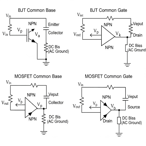
The basic operation with ideal bias at the emitter of this BJT we require some biasing arrangement. So, that the DC current need to be supported at the base we require a DC voltage.
Detailed Explanation
This section explains the fundamental operating principles of both common base (BJT) and common gate (MOSFET) amplifiers. It discusses the importance of proper biasing to maintain the operating point and allow for effective signal amplification. The input signal is applied at the emitter for BJT and at the source for MOSFET while the output is taken from the collector or drain respectively. It also emphasizes the concept of DC and AC interactions, noting how coupling capacitors allow AC signals to pass through while blocking DC.
Examples & Analogies
Think of biasing like adjusting the volume of a radio to a comfortable level before tuning into your favorite station. If the volume is too low (poor biasing), you won’t hear anything; too high, and the sound might distort. The ideal bias point ensures you can hear the signal clearly without any distortion.
Biasing Techniques for Common Base Amplifier
Chapter 4 of 5
🔒 Unlock Audio Chapter
Sign up and enroll to access the full audio experience
Chapter Content
Here how do you practically make this bias. Suppose you do have the BJT main BJT is here and here either we can put another transistor say NPN transistor having a meaningful bias at its base.
Detailed Explanation
This segment discusses how to effectively bias a common base amplifier using additional circuits or transistors to create a stable operating point. It outlines designs where another transistor is used for biasing, explaining how these devices support necessary DC levels without affecting AC signal paths. The importance of ensuring high output impedance while providing sufficient current for the main transistor is also stressed.
Examples & Analogies
Consider your car’s navigation system. Just like the system needs a good signal (biasing) to provide accurate directions, the common base amplifier requires proper biasing to function effectively. If the navigation system isn’t calibrated correctly, you may find yourself lost—this is similar to how poor biasing can affect circuit performance.
Biasing Techniques for Common Gate Amplifier
Chapter 5 of 5
🔒 Unlock Audio Chapter
Sign up and enroll to access the full audio experience
Chapter Content
The biasing scheme of the common gate on the other hand here we are having the main transistor. So, we do have the main transistor and then at the source side we do have.
Detailed Explanation
In this part, similar to the common base amplifier, the common gate amplifier is discussed regarding effective biasing solutions. The focus is on ensuring the gate voltage is appropriately set while providing stable operating conditions for the MOSFET. The text again emphasizes the need for matching currents and maintaining balance between source and drain biasing, reiterating that incorrect biasing can lead to operational issues.
Examples & Analogies
Think of setting up a new thermostat in your home. If the sensors (bias conditions) are set wrong, your house may become too hot or too cold (operational issues). Just as you want your thermostat to function properly to maintain a comfortable environment, ensuring correct biasing of your common gate amplifier is crucial for optimal performance.
Key Concepts
-
Common Base Configuration: Used for BJT amplifiers, primarily as a current buffer.
-
Common Gate Configuration: Employed in MOSFET amplifiers for similar current buffering.
-
Loading Effect: The influence of output impedance of one stage on input impedance of the next stage affecting gain and bandwidth.
-
Biasing: Establishing the DC operating point for transistors to ensure proper function.
-
Small Signal Analysis: The technique used for analyzing the amplifier's parameters under small input fluctuations.
Examples & Applications
The common base amplifier can be used in RF applications where high-frequency performance is critical due to its low input capacitance.
In a common gate amplifier, increasing the source voltage hence reducing the gate-source voltage can enhance the current flowing from drain to source.
Memory Aids
Interactive tools to help you remember key concepts
Rhymes
In a buffer that’s common base, Stability finds its place.
Stories
In a bustling electronics town, a wise old amplifier named 'Common Base' helped everyone buffer their signals without dropping the ball.
Memory Tools
Remember 'B' for Base and 'G' for Gate to keep amplifiers in good state!
Acronyms
B.B.C.G. stands for Basic Biasing of Common Gain
The essential roles of biasing in amplifier performance.
Flash Cards
Glossary
- Common Base Amplifier
A configuration of a BJT amplifier wherein the base terminal is common to both input and output circuits.
- Common Gate Amplifier
A configuration of a MOSFET amplifier where the gate terminal is common to both input and output circuits.
- Biasing
The process of setting a transistors' DC operating point.
- Voltage Gain
The ratio of output voltage to input voltage in an amplifier.
- Input Impedance
The impedance seen by the source from the input terminal of the amplifier.
- Output Impedance
The impedance presented by the amplifier at its output terminal.
Reference links
Supplementary resources to enhance your learning experience.