
Common Emitter Amplifier (Contd.) Design Guidelines (Part B)
Enroll to start learning
You’ve not yet enrolled in this course. Please enroll for free to listen to audio lessons, classroom podcasts and take practice test.
Interactive Audio Lesson
Listen to a student-teacher conversation explaining the topic in a relatable way.
Maximizing Gain
🔒 Unlock Audio Lesson
Sign up and enroll to listen to this audio lesson

Welcome back! Today, let's explore how to maximize gain in a Common Emitter amplifier. Can anyone tell me what's the importance of gain in amplifier design?

Gain allows the amplifier to boost weak signals to a usable level, right?
Exactly! The primary goal in amplifier design is often to maximize voltage gain. We need to design to accommodate the desired gain without exceeding limits, such as the maximum gain our circuit can handle, which we've established can be around 230.

What happens if we need a gain that's less than that?
Great question! If the specified gain is lower than the maximum, we can adjust our resistors, but we need to make sure the bias point stability remains intact.

What’s the impact of ignoring certain components like bypass capacitors?
Bypassing affects bias stability! It’s essential to consider each component’s effect on the overall design. Remember, we can partially bypass resistors to help achieve the proper gain while maintaining stability. Now let's recap: A suitable design ensures maximum gain without sacrificing stability.
Cascading Amplifiers
🔒 Unlock Audio Lesson
Sign up and enroll to listen to this audio lesson

Now, let's discuss cascading amplifiers. Can anyone tell me why we might want to cascade stages?

To achieve a higher overall gain, right?
Correct! By cascading two Common Emitter amplifiers, we can multiply their gains. For instance, if each stage has a gain of 253, the total gain can be much higher!
How do we calculate the overall gain for cascaded amplifiers?
The overall gain is the product of each stage's gain modified by the loading effect from the resistor configurations. It's important to analyze the output and input resistances to determine the attenuation.
What if the input resistance of the second stage is too low?
It can lead to decreased overall gain due to excessive loading. Always keep in mind the input and output resistance interactions when cascading. Let's summarize: Cascading amplifiers effectively multiplies gain but requires careful consideration of their resistances.
Stability and Design Adjustments
🔒 Unlock Audio Lesson
Sign up and enroll to listen to this audio lesson
Finally, let’s focus on design adjustments and the stability of the operating point. Why is this important?
It ensures consistent performance despite component variations, right?
Exactly! Using appropriately sized resistors helps ensure the operating point remains stable across varying beta values. Would anyone like to dive deeper into resistor sizing and bypassing?
How do we determine resistor values?
By understanding the gain requirements and calculating accordingly. For instance, if we want a 20 dB gain and have a resistor ratio to maintain point stability, careful consideration is critical. Remember never to ignore any component in the circuit!
So partial bypassing can help achieve that, correct?
Yes! Partial bypassing balances gain and stability effectively. In summary, focus on the implications of each adjustment we make regarding bias and stability.
Introduction & Overview
Read summaries of the section's main ideas at different levels of detail.
Quick Overview
Standard
The section elaborates on design strategies to maximize gain and output swing while maintaining stability and performance. It explains how to adjust amplifier circuits based on required performance parameters and introduces techniques for cascading amplifiers to achieve higher overall gain.
Detailed
The chapter section delves into the design guidelines for Common Emitter (CE) amplifiers, emphasizing the goals of maximizing voltage gain and output swing while ensuring power dissipation stays within practical limits. Important parameters include the supply voltage (V_C) and gain limits under various configurations. The section also covers techniques for adjusting gain through resistor configurations, the concept of bypassing resistors partially to maintain bias point stability, and the methodology of cascading multiple amplifier stages for enhanced overall gain. Examples and detailed explanations illustrate these points, highlighting the significance of bias stability and resistor values in amplifier design.
Youtube Videos

Audio Book
Dive deep into the subject with an immersive audiobook experience.
Maximizing Gain and Output Swing
Chapter 1 of 5
🔒 Unlock Audio Chapter
Sign up and enroll to access the full audio experience
Chapter Content
Welcome back after this short break and let me continue the Design Guidelines for CE Amplifier. So far we have discussed about the design guidelines where our main objective is to maximize the gain, voltage gain right. And, also the output swing we like to maximize and the power dissipation probably it is a given value. And, this maximization of output swing of course, it is decided by the V_CC. Likewise, the maximization of the gain is also decided by this V_CC and thermal equivalent voltage and of course, the output swing.
Detailed Explanation
This chunk discusses the primary goals when designing a Common Emitter Amplifier (CE amplifier). The two major objectives are maximizing the voltage gain and output swing while managing power dissipation, which is often predetermined. The output swing is crucial for ensuring that the amplifier can handle the desired signal variations without distortion, and it directly depends on the supply voltage (V_CC) and thermal considerations. Understanding these elements is essential for successfully designing an amplifier that meets specific requirements.
Examples & Analogies
Think of designing a speaker system. You want the sound (gain) to be loud and clear (output swing), but you also have to consider how much power (dissipation) the system can handle without overheating. Just like adjusting the volume and power limits of a speaker, adjusting V_CC helps control how much 'amplification' you can achieve in your amplifier design.
Designing for Lower Gains
Chapter 2 of 5
🔒 Unlock Audio Chapter
Sign up and enroll to access the full audio experience
Chapter Content
So, typically we like to keep the output swing towards its maximum as much as possible, but definitely there may be a requirement where say we require only a 20 gain, unnecessarily we will not be looking for say 230 gain. So, in case if this gain is specified and if it is less than this limit, then what may be the design guidelines or design procedure to achieve that.
Detailed Explanation
This chunk explains that while high gains are often desirable, there are scenarios where a lower gain (like 20) is sufficient. The challenge arises when designing the circuit to achieve this specified lower gain without compromising the overall performance or stability. The design considerations will vary based on the desired gain, and specific design guidelines can be followed to ensure a stable operating point despite reduced amplification.
Examples & Analogies
Imagine you are tuning a radio. Sometimes, you want a signal just good enough to listen to music (lower gain) without blasting it to maximum volume. This is similar to designing an amplifier for a specified gain—measuring and setting the right levels to achieve clarity without distortion or unnecessary amplification.
Bypassing Resistors to Enhance Gain
Chapter 3 of 5
🔒 Unlock Audio Chapter
Sign up and enroll to access the full audio experience
Chapter Content
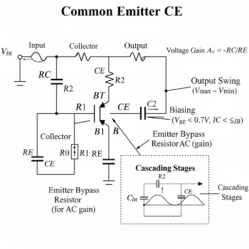
So, what may be the remedy for that instead of completely ignoring the R_E or instead of completely bypassing this R_E, what you can do we can partially bypass this resistor?
Detailed Explanation
In this part, the discussion revolves around mitigating issues that arise when designing an amplifier circuit. Instead of bypassing the Emitter Resistor (R_E) completely, which could lead to gain instability, the design can include a partial bypass. This strategy helps maintain a stable operating point by ensuring that some resistance remains in the circuit, which stabilizes the voltage across the transistor and prevents large variations in gain due to changes in β (beta), a parameter that describes the transistor's amplification capability.
Examples & Analogies
Imagine a water faucet. If you partially close the faucet (partial bypass), you can control the flow of water better, compared to fully opening or fully closing it which could lead to overflow or no flow at all. Similarly, partially bypassing R_E allows you to control the gain better and ensure smooth operation of the amplifier.
Cascading Amplifiers for Higher Gain
Chapter 4 of 5
🔒 Unlock Audio Chapter
Sign up and enroll to access the full audio experience
Chapter Content
So, the next thing is that in case if we are looking for a circuit having this gain, which is higher than the limit of the maximum gain... So, there are two possibilities probably we can replace this resistor by an active device... cascade to an amplifier to get total gain maybe multiplication of the 2 individual stages gain.
Detailed Explanation
Cascading refers to connecting multiple amplifier stages in sequence to increase overall gain. When seeking a gain higher than what a single CE amplifier can provide, designers often resort to connecting two or more amplifier circuits together. This method allows the total gain of the system to be the product of each stage's gain, effectively multiplying their amplification capabilities. However, it is essential to calculate the resistances properly to ensure that the connection between the two stages does not negatively impact performance.
Examples & Analogies
Think of a relay team in a race. Each runner (amplifier stage) has their own strengths, but when combined, they can cover more distance in less time (gain). If each runner does well, the entire team benefits, and that's the concept behind cascading amplifiers to achieve much higher overall gain.
Importance of Input and Output Resistance
Chapter 5 of 5
🔒 Unlock Audio Chapter
Sign up and enroll to access the full audio experience
Chapter Content
Now, if I replace these 2 amplifiers by their corresponding model for signal, small signal model... So, the voltage coming here is the A × v_1; this v that voltage it is only here.
Detailed Explanation
This section emphasizes the importance of understanding how the input and output resistances of each amplifier stage influence overall circuit behavior. In a cascaded configuration, the output resistance of the first amplifier can affect the input resistance of the second. One must carefully account for these resistances when calculating overall gain and ensuring signal integrity. Properly matching these resistances can maximize efficiency and reduce signal loss.
Examples & Analogies
Imagine a chain where each link represents an amplifier stage. If one link (output resistance) is too heavy or large, it slows down the entire chain (overall gain). By making sure each link is appropriately sized (matching resistances), the chain moves smoothly and efficiently, much like ensuring signal flow between cascaded amplifiers.
Key Concepts
-
Gain: The measure of amplification in an amplifier, influencing how well a weak signal can be amplified.
-
Output Swing: The range of output voltage levels an amplifier can produce, critical for linearly amplifying signals.
-
Cascading: A method of combining multiple amplifier stages to increase gain, but must be managed to prevent signal degradation.
Examples & Applications
If an amplifier has a gain of 200 and is cascaded with another amplifier of the same gain, the overall gain can reach 40000 when accounting for load effects.
If you select resistor values strategically, such as a 1 kΩ resistor and a bypass capacitor with a capacitance of 10 µF, it supports achieving a balanced gain of 20 without compromising stability.
Memory Aids
Interactive tools to help you remember key concepts
Rhymes
Gain high, swing wide, keep bias in stride; stable designs for circuits that glide.
Stories
Imagine building a tower; each floor is an amplifier stage. To reach great heights, you must ensure each stage is robust and not swayed by winds—this is your bias stability.
Memory Tools
Remember 'GSC' - Gain, Stability, Cascading. Each concept strengthens amplifier design.
Acronyms
C.E.A.M
Common Emitter
Amplifier Maximization. Think of it as your guide to designing effective amplifiers.
Flash Cards
Glossary
- Common Emitter Amplifier
An amplifier configuration that provides significant voltage gain, using the emitter terminal as a reference point.
- Voltage Gain
The ratio of output voltage to input voltage, expressed in decibels.
- Bypass Capacitor
A capacitor used in an amplifier to prevent AC signals from passing through a resistor, thus maintaining higher gain.
- Cascading
Connecting multiple amplifier stages in sequence to increase overall gain.
- Bias Point Stability
The consistency of the amplifier's operating point against variations in device parameters.
Reference links
Supplementary resources to enhance your learning experience.