
Implementation Configurations
Enroll to start learning
You’ve not yet enrolled in this course. Please enroll for free to listen to audio lessons, classroom podcasts and take practice test.
Interactive Audio Lesson
Listen to a student-teacher conversation explaining the topic in a relatable way.
Voltage Mode Buffers
🔒 Unlock Audio Lesson
Sign up and enroll to listen to this audio lesson

Today, we're going to explore voltage mode buffers. Can anyone tell me what key characteristics a voltage mode buffer should have?

I think the output resistance should be low, right?
Yes, that's correct! We want the output resistance low to ensure minimal loading effect. What about the input resistance?

It should be high to prevent signal loss.
Excellent! Remember, we want high input resistance and low input capacitance to maintain the cutoff frequency. Can anyone share what kind of configurations we use for these buffers?

Common collector for BJTs and common drain for MOSFETs?
That's right! Now let's summarize: low output resistance, high input resistance, and low input capacitance. Great job!
Current Mode Buffers
🔒 Unlock Audio Lesson
Sign up and enroll to listen to this audio lesson

Next, let's discuss current mode buffers. What do we need to remember about the output resistance for these buffers?

It should be high to avoid loading effects!
Absolutely! And how about the input resistance?
It should be low to let the input current flow easily.
Exactly! The current gain should ideally be around 1 as well. Can anyone name the buffer configurations used in BJTs and MOSFETs?
Common base for BJTs and common gate for MOSFETs.
Well done! Remember, the balance between input and output resistance in current mode is crucial for effective signal propagation.
Importance of Buffers
🔒 Unlock Audio Lesson
Sign up and enroll to listen to this audio lesson
Now, let's reflect on why buffers are important in amplifier circuits. Why do we use them during cascading?
To prevent bandwidth loss and signal attenuation?
Exactly! Buffers help improve the bandwidth and gain of cascaded amplifiers. Can anyone summarize the important features of voltage and current mode buffers?
For voltage mode, we need low output resistance, high input resistance, and low input capacitance. For current mode, we need high output resistance and low input resistance.
Great summary! Remember these features, as they are key to designing effective audio and signal processing circuits.
Introduction & Overview
Read summaries of the section's main ideas at different levels of detail.
Quick Overview
Standard
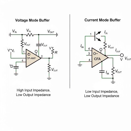
The section details the necessary characteristics of buffers used in voltage and current mode amplifiers, explaining how their configurations, namely common collector and common base for BJTs and common drain and common gate for MOSFETs, affect performance.
Detailed
Implementation Configurations
This section highlights the importance of buffer configurations in both voltage and current mode amplifiers. Key features discussed include:
- Voltage Mode Buffers: For these buffers, the output resistance should be minimized, while the input resistance is maximized, and input capacitance should also be kept low to preserve cutoff frequency. The voltage gain should ideally be around 1. These features are typically achieved using common collector configurations in BJTs and common drain configurations in MOSFETs.
-
Current Mode Buffers: In contrast, for current mode applications, the output resistance should be maximized to avoid loading effects, while the input resistance should be minimized to ensure proper signal propagation. Current gain should also remain close to 1. The common base configuration for BJTs and common gate configuration for MOSFETs are used to achieve these features.
Ultimately, buffers play a crucial role in improving the bandwidth and gain of cascaded amplifiers, thereby enhancing overall circuit performance.
Youtube Videos

Audio Book
Dive deep into the subject with an immersive audiobook experience.
Voltage Mode Buffer Requirements
Chapter 1 of 4
🔒 Unlock Audio Chapter
Sign up and enroll to access the full audio experience
Chapter Content
The output resistance of this buffer should be as small as possible. Conversely, the input resistance of this buffer should be as high as possible. The input capacitance should also be minimized to avoid affecting the upper cutoff frequency. Ideally, the voltage gain of this circuit should be around 1.
Detailed Explanation
In a voltage mode buffer configuration, we want to achieve several key characteristics. First, the output resistance should be low, meaning the buffer can deliver power effectively to the next stage of the circuit without losing voltage. Second, the input resistance should be high to minimize the load it places on the preceding stage, allowing more signal to pass through. Additionally, we want to keep the input capacitance low to ensure that the circuit can respond quickly to changes in the input signal. Lastly, having a voltage gain close to 1 indicates that the buffer is amplifying the signal without significant alteration.
Examples & Analogies
Think of the voltage mode buffer as a well-designed relay in a plumbing system. The low output resistance ensures that the water flows easily from one pipe to another (the next stage), while the high input resistance means the first pipe is not significantly slowed down by the relay. The small input capacitance ensures that the relay responds quickly to changes in water pressure (signal changes), and having a gain close to 1 is like ensuring that the water pressure stays the same as it flows through the relay.
Common Collector/Common Drain Configurations
Chapter 2 of 4
🔒 Unlock Audio Chapter
Sign up and enroll to access the full audio experience
Chapter Content
These requirements can be achieved using different circuit configurations. For BJTs, the common collector configuration is used. For MOS transistors, the common drain configuration serves the same purpose.
Detailed Explanation
To implement the desired characteristics of a voltage mode buffer, we typically use specific circuit configurations. For Bipolar Junction Transistors (BJTs), we use a common collector configuration, commonly known as an emitter follower, which allows the input signal to follow the output effectively. For MOSFETs, we use a similar configuration called the common drain. Both configurations help in achieving low output resistance, high input resistance, and maintaining the necessary voltage gain.
Examples & Analogies
Imagine a series of relay stations that help transmit messages. The common collector configuration is like a station that allows messages to flow through without losing clarity—similar to how an emitter follower works. If we consider MOSFETs, the common drain is like a similar but slightly modified station that’s better suited for another network type, ensuring that the messages reach their destination with minimal distortion and high integrity.
Current Mode Buffer Requirements
Chapter 3 of 4
🔒 Unlock Audio Chapter
Sign up and enroll to access the full audio experience
Chapter Content
For current mode amplifiers, the output resistance should be as high as possible to avoid loading effects, while the input resistance should be low to allow input current to flow easily without hindrance. The current gain should ideally be around 1.
Detailed Explanation
In contrast to voltage mode buffers, current mode amplifiers require different buffer characteristics. Here, we want the output resistance to be high so that it does not draw too much current from the previous stage, avoiding loading effects that could distort the signal. The input resistance should be low to allow current to flow freely into the buffer, promoting signal integrity. Finally, maintaining a current gain close to 1 ensures that the amplifier does not significantly attenuate the signal.
Examples & Analogies
Consider the current mode buffer similar to a fast track for vehicles. The high output resistance is like a lane that lets cars from previous roads merge without creating a traffic jam, which could slow everything down. The low input resistance corresponds to an easy entry point where vehicles can flow onto the track without obstacles. Ensuring a current gain of about 1 means that the track doesn’t change the speed at which vehicles are traveling too dramatically, keeping everything running smoothly.
Common Base/Common Gate Configurations
Chapter 4 of 4
🔒 Unlock Audio Chapter
Sign up and enroll to access the full audio experience
Chapter Content
Current mode buffers can be implemented using a common base configuration for BJTs and a common gate configuration for MOSFETs.
Detailed Explanation
To meet the requirements of current mode buffers, specific configurations are adopted. The common base configuration, typically used for BJTs, allows the circuit to effectively handle varying current levels while maintaining the necessary low input resistance. For MOSFETs, the common gate configuration serves a similar function, enabling efficient signal processing in a current mode application while accommodating high output resistance. These configurations are crucial for achieving the optimal performance of current mode amplifiers.
Examples & Analogies
Think of the common base and common gate configurations as specialized entry points in a theme park. The common base is like a special access gate that allows people (current) to enter seamlessly with very little friction, while the common gate is a different setup that allows for quick access without delays. Both ensure that visitors flow through efficiently, facilitating a strong experience without bottlenecks—much like ensuring proper signal flow in an amplifier configuration.
Key Concepts
-
Output Resistance: The resistance looking into the output of the buffer, ideally low for voltage mode and high for current mode.
-
Input Resistance: High for voltage mode buffers to avoid loading; low for current mode to facilitate current flow.
-
Input Capacitance: Should be minimized in voltage mode to maintain cutoff frequencies.
-
Voltage Gain: Ideally around 1 for both voltage and current mode amplifiers.
Examples & Applications
Using a common collector buffer in an audio circuit to maintain signal integrity.
Implementing a common gate buffer in a sensor circuit to ensure effective signal transfer.
Memory Aids
Interactive tools to help you remember key concepts
Rhymes
For voltage mode, keep resistance low, high input's the way, let the signal flow.
Stories
Imagine two friends: Volt and Curran. Volt likes low resistance for dances, while Curran needs high support to run smoothly in a race.
Memory Tools
V.E.L.C. (Voltage = Low Output, Capacitor Low; Current = High Output, Low Input).
Acronyms
B.I.G. (Buffers Improve Gain) to remember the importance of buffers in amplifier design.
Flash Cards
Glossary
- Voltage Mode Buffer
A buffer circuit designed to amplify voltage with specific input and output resistance characteristics.
- Current Mode Buffer
A buffer circuit that operates primarily on current and is designed to optimize current characteristics.
- Common Collector
BJT configuration used for voltage mode buffering; offers low output resistance.
- Common Drain
MOSFET configuration used for voltage mode buffering; serves a similar function to common collector in BJTs.
- Common Base
BJT configuration used for current mode buffering; provides high output resistance.
- Common Gate
MOSFET configuration suitable for current mode buffering with high output resistance.
Reference links
Supplementary resources to enhance your learning experience.