
Necessary Features of the Buffer
Enroll to start learning
You’ve not yet enrolled in this course. Please enroll for free to listen to audio lessons, classroom podcasts and take practice test.
Interactive Audio Lesson
Listen to a student-teacher conversation explaining the topic in a relatable way.
Essential Resistance Characteristics for Buffers.
🔒 Unlock Audio Lesson
Sign up and enroll to listen to this audio lesson

Today we will discuss the necessary features of the buffer. Can someone tell me why output resistance is significant for a voltage mode buffer?

Is it because we want to minimize loading effects?
Exactly! We want the output resistance to be as low as possible. What about input resistance?

It should be high, right? To keep the signal from being compromised.
Correct! Now, let's remember the acronym 'LOHI' to recall: Low Output, High Input. Lastly, why do we want the input capacitance to be low?

We need to avoid affecting the cutoff frequency!
Precisely! Low input capacitance helps maintain the integrity of the circuit's performance.
In summary, for voltage mode buffers, we need low output resistance, high input resistance, and low input capacitance. Remember 'LOHI'!
Voltage Gain Considerations.
🔒 Unlock Audio Lesson
Sign up and enroll to listen to this audio lesson

Now let’s talk about gain. What gain should we ideally target in voltage mode buffers?

It should be around 1?
Exactly! A voltage gain of approximately 1 helps in maintaining the signal level. Why do you think maintaining this gain is crucial?
To avoid signal attenuation and ensure proper amplification.
Right again! This ensures efficient performance when cascading amplifiers. Let’s now connect this back to circuit configurations.
Current Mode Buffers.
🔒 Unlock Audio Lesson
Sign up and enroll to listen to this audio lesson
Moving to current mode amplifiers, what do you think the requirements for the buffer are?
We would need high output resistance to prevent loading effects.
Correct! And what about input resistance?
It should be low to efficiently handle input current.
Exactly! We want to ensure smooth signal propagation. Now can someone tell me about the common configurations for these buffers?
For BJTs, we use common base, and for MOSFETs, it's common gate.
Great! Remember to associate these configurations with their buffer requirements.
Cascading Amplifiers.
🔒 Unlock Audio Lesson
Sign up and enroll to listen to this audio lesson
Finally, how do buffers help when cascading amplifiers?
They help to maintain bandwidth and gain throughout the stages.
Absolutely! They prevent the limitations that can occur with just common emitter configurations. Can you summarize the features we've discussed today?
For voltage mode, we need low output resistance, high input resistance, low input capacitance, and around a gain of 1!
And for current mode, it’s high output resistance, low input resistance, and configurations like common base or gate!
Fantastic summary! Great job today, everyone!
Introduction & Overview
Read summaries of the section's main ideas at different levels of detail.
Quick Overview
Standard
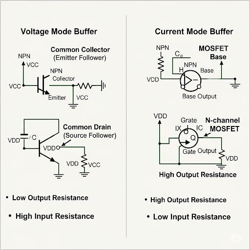
This section covers the necessary features of buffers used in voltage and current mode amplifiers, detailing desired resistances, capacitance, and voltage/current gains for optimal performance in circuit applications.
Detailed
In this section, we explore the crucial features that buffers must possess to operate effectively in voltage mode and current mode amplifiers. For a voltage mode buffer, it is essential for the output resistance to be as low as possible to minimize loading effects, while the input resistance should be as high as possible to maintain signal integrity. Additionally, the input capacitance must be minimized to prevent distortion of the cutoff frequency, and a voltage gain of approximately 1 is preferred. Configurations like common collector (for BJT) and common drain (for MOSFET) are typically employed to meet these requirements. Conversely, for current mode amplifiers, the qualities are inverted: a high output resistance is desirable to avoid loading effects, and a low input resistance is preferred to allow effective signal transfer. This is implemented through common base (for BJT) or common gate (for MOSFET) configurations. The presence of buffers can help mitigate limitations in bandwidth and gain when cascading amplifiers, underscoring their significance in achieving desired amplifier characteristics.
Youtube Videos

Audio Book
Dive deep into the subject with an immersive audiobook experience.
Output Resistance Minimum
Chapter 1 of 5
🔒 Unlock Audio Chapter
Sign up and enroll to access the full audio experience
Chapter Content
So, on the other hand the input resistance of this buffer should be as high as possible. So, quote and unquote high and then input capacitance again it should be as small as possible. So, that the cutoff frequency should not get upper cutoff frequency should not get affected. So, again here it is quote and unquote low.
Detailed Explanation
This chunk talks about the necessary characteristics for a buffer amplifier, especially focused on the output and input resistances and capacitance. The output resistance should be low to allow for better current transfer, while the input resistance needs to be high, ensuring minimal signal loss and maximum signal integrity. Additionally, a low input capacitance is essential for maintaining the cutoff frequency of the circuit, preventing unwanted changes in the frequency response.
Examples & Analogies
Think of a buffer amplifier like a well-designed water pipe system. A low output resistance is like using wider pipes at the end where water flows out, allowing easy access to the water without much pressure drop. A high input resistance acts like a narrow entrance to a reservoir that allows water to build up without losing much of it, ensuring a stable supply without wasting resources.
Voltage Gain Requirement
Chapter 2 of 5
🔒 Unlock Audio Chapter
Sign up and enroll to access the full audio experience
Chapter Content
And, then the voltage gain of this circuit preferably it should not be very small. So, we should be rather happy if it is in the order of 1 ok.
Detailed Explanation
In addition to resistances and capacitance, the voltage gain of the buffer circuit is also critiqued. It is beneficial for the gain to be close to 1. This means that the output voltage reflects the input voltage without significant amplification or attenuation, maintaining the original signal quality. A gain significantly less than 1 could indicate that the buffer is not effectively transferring the signal.
Examples & Analogies
Imagine a speaker connected to a music source. If the volume is turned up too high (gaining more than 1), the sound might distort, and if it's too low (gaining less than 1), you might not hear anything. A gain of 1 represents the ideal balance, where the music from the source is heard clearly and accurately through the speaker.
Circuit Configurations for Voltage Buffers
Chapter 3 of 5
🔒 Unlock Audio Chapter
Sign up and enroll to access the full audio experience
Chapter Content
Now, this kind of requirement it is essentially it will be obtained by different circuit configuration namely; common collector if it is implemented by BJT. If it is implemented by MOS transistor it will be common drain; which means that this buffer particularly for voltage mode amplifier cascading this buffer it will be implemented by common collector or common drains stage.
Detailed Explanation
This chunk discusses the specific circuit configurations used to achieve the desired buffer features. For bipolar junction transistors (BJTs), the common collector configuration is typically employed, while for MOSFETs, the common drain configuration is used. These configurations allow for low output resistance and high input resistance, fulfilling the design goals we discussed earlier.
Examples & Analogies
Think of circuit configurations like different types of bridges designed for vehicles. A common collector setup is akin to a sturdy bridge built for heavy trucks: it allows for direct and efficient passage without much resistance. On the other hand, a common drain is like a pedestrian bridge that provides a smooth, easy pathway for foot traffic, ensuring it too handles its load gracefully.
Buffer Characteristics for Current Mode Amplifiers
Chapter 4 of 5
🔒 Unlock Audio Chapter
Sign up and enroll to access the full audio experience
Chapter Content
So, this is the required buffer for current mode amplifier cascading. What we are looking for it is that output resistance for this case to avoid the loading effect, output resistance particularly the resistance wise, it should be as high as possible quote an unquote high. And, then input resistance it is the dual effect to avoid the loading effect the input current should be consumed by this circuit without any problem, so, that we can get the signal propagating there.
Detailed Explanation
In current mode amplifiers, the required buffer characteristics are quite distinct from voltage mode amplifiers. The output resistance should be high to prevent loading effects on the circuit, which could decrease the performance of the amplifier. Simultaneously, the input resistance should be low enough to allow for adequate current consumption without significant voltage drop.
Examples & Analogies
Consider this like a relay race where one runner passes the baton to the next. If the next runner (output of the buffer) is unable to accept the baton (high output resistance), the race can falter. Meanwhile, if the current is too high on the first runner (low input resistance), it can lead to confusion and slow down the race. In this scenario, both runners need to manage their exchanges carefully to maintain speed and efficiency.
Conclusion on Buffer Features
Chapter 5 of 5
🔒 Unlock Audio Chapter
Sign up and enroll to access the full audio experience
Chapter Content
So, I think in the next class we will be able to discuss more detail about those different kinds of configuration and we will discuss about how they can be design that is all.
Detailed Explanation
The section concludes by summarizing the key points about buffer features for both voltage and current mode amplifiers. It emphasizes the importance of choosing appropriate configurations to enhance performance and maintain desired characteristics during cascading operations. Understanding these features is foundational for designing efficient amplifiers that meet specific needs.
Examples & Analogies
Think of designing these buffer amplifiers as planning for different types of events. For a music concert, a sound engineer needs to ensure the right speaker setups (configurations) based on the venue (amp type) to maintain an audible and enjoyable experience. Similarly, by understanding the buffer features, engineers can ensure optimal performance in amplifiers.
Key Concepts
-
Output Resistance: Should be low in voltage buffers to minimize loading.
-
Input Resistance: Should be high in voltage buffers to maintain signal integrity.
-
Input Capacitance: Should be low in buffers to prevent cutoff frequency distortion.
-
Voltage Gain: Desired to be close to 1 in voltage mode buffers.
-
Buffer Configurations: Common collector/common drain for voltage mode, common base/common gate for current mode.
Examples & Applications
A common collector amplifier is used as a buffer in audio circuit designs to interface between high-impedance sources and low-impedance loads.
In RF amplifiers, common gate configurations are used to achieve necessary current mode buffering while maintaining signal fidelity.
Memory Aids
Interactive tools to help you remember key concepts
Rhymes
Buffers keep signals intact, low resistance is a fact.
Stories
Imagine a vast river where low dams let water flow freely, ensuring no obstruction as it moves downstream just like low output resistance buffers allow signals to travel seamlessly.
Memory Tools
LOHI: Low Output, High Input, keep Capacitance low, and Voltage gain near one in buffer flow.
Acronyms
BICE
Buffers Input Capacitance Extremely low.
Flash Cards
Glossary
- Output Resistance
The resistance seen by the load connected to the output of a buffer; low values are desired to minimize loading effects.
- Input Resistance
The resistance that the input of a buffer presents to the incoming signal; high values are necessary to prevent signal loss.
- Input Capacitance
The capacitance at the input of a buffer, which should be minimized to prevent distortion of cutoff frequencies.
- Voltage Gain
The ratio of output voltage to input voltage; a gain near 1 is preferred in voltage buffers for optimal signal integrity.
- Common Collector
A BJT configuration that allows for high input resistance and low output resistance, suitable for voltage buffers.
- Common Drain
A MOSFET configuration similar to common collector, suited for voltage mode buffering.
- Common Base
A BJT configuration used in current mode buffers characterized by high output resistance.
- Common Gate
A MOSFET configuration that supports low input resistance, suitable for current mode buffers.
Reference links
Supplementary resources to enhance your learning experience.