
Manufacturing Cost
Interactive Audio Lesson
Listen to a student-teacher conversation explaining the topic in a relatable way.
Introduction to Manufacturing Costs
🔒 Unlock Audio Lesson
Sign up and enroll to listen to this audio lesson

Today, we are exploring the manufacturing costs related to FinFET technologies. Manufacturing costs have risen due to advanced techniques. Can anyone tell me why we might see increased expenses?

Is it because the technology is new and requires special equipment?
Exactly, Student_1! New technologies often require state-of-the-art equipment. Specifically, FinFETs use 3D patterning, which adds complexity. Let's dig deeper. What do you think 3D patterning entails?

I think it means they are layering materials in a more complex way than before?
Great point, Student_2! 3D patterning allows for better scaling of transistors, but it also results in higher production costs due to additional steps in manufacturing. Let’s summarize this part: manufacturing costs are rising primarily due to the complexity of 3D patterning techniques.
The Role of Lithography
🔒 Unlock Audio Lesson
Sign up and enroll to listen to this audio lesson

Now, let’s shift our focus to lithography. Who can explain what lithography is in the context of semiconductor manufacturing?

It’s the process used to etch designs onto the semiconductor material, right?
Correct, Student_3! Lithography is crucial for defining transistor shapes at nanometer precision. The FinFET process requires highly advanced lithography technology, which is more expensive than traditional methods. Can anyone see the connection to costs here?

If it requires more advanced tools, it must cost more to operate those machines...
Absolutely, Student_4! That leads us to the point: the enhanced lithography needed for FinFET manufacturing directly contributes to increased costs.
Overall Cost Impact
🔒 Unlock Audio Lesson
Sign up and enroll to listen to this audio lesson
Let's summarize what we've learned about costs. How do you think these factors combined affect the overall production of FinFET devices?
I guess with both 3D patterning and advanced lithography being expensive, it makes the whole process costlier.
Exactly, Student_2! The additional costs from both complexity and advanced tools lead to higher prices for FinFET-based products. In industry terms, we need to consider the balance between performance and cost. Can anyone suggest why this balance is critical?
It impacts how profitable a new product can be...
Well said, Student_1! Profitability is vital. As we conclude, remember that rising manufacturing costs due to FinFET complexities pose challenges for developers aiming to introduce innovative products.
Introduction & Overview
Read summaries of the section's main ideas at different levels of detail.
Quick Overview
Standard
The section discusses the challenges associated with manufacturing costs of FinFETs, particularly focusing on the increased expenses stemming from 3D patterning and advanced lithography methods. It highlights how these factors impact the overall cost of semiconductor production within system-on-chip (SoC) designs.
Detailed
Manufacturing Cost in FinFET Technologies
The emergence of FinFET technology has significantly enhanced the performance and efficiency of semiconductor devices; however, it has also introduced challenges related to manufacturing costs.
Key Points:
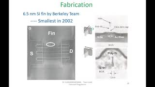
- 3D Patterning: The shift from traditional planar designs to FinFET requires advanced 3D patterning techniques that enhance transistor performance. This complexity leads to increased fabrication costs.
- Lithography: Manufacturing FinFETs demands sophisticated lithography tools, necessitating precise fabrication methods that add to capital expenditure. This intricate process is not only time-consuming but also calls for higher investments in equipment that can operate at nanometer scales.
- Overall Impact: These factors collectively raise the overall manufacturing cost of integrated circuits, making the commercial production of FinFET-based SoC devices more expensive compared to conventional technologies.
Understanding these cost dynamics is crucial for stakeholders in the semiconductor industry as they balance performance improvements with budgetary constraints.
Youtube Videos


Audio Book
Dive deep into the subject with an immersive audiobook experience.
Introduction to Manufacturing Costs in FinFET Technology
Chapter 1 of 2
🔒 Unlock Audio Chapter
Sign up and enroll to access the full audio experience
Chapter Content
Manufacturing Cost
● 3D patterning and lithography increase fabrication expense.
Detailed Explanation
Manufacturing costs in FinFET technology are primarily affected by two key processes: 3D patterning and lithography. These processes are essential for creating the intricate structures needed in FinFETs, which are crucial for their performance and efficiency. Because these methods require advanced equipment and technologies, they can significantly raise the overall costs of producing FinFET devices compared to traditional planar transistors.
Examples & Analogies
Think of 3D patterning and lithography like a complex art project. Just as an artist might need expensive tools and specific materials to create a detailed sculpture, semiconductor manufacturers need sophisticated machinery and processes to create intricate transistors, which increases their production costs.
Impact of Increased Manufacturing Costs
Chapter 2 of 2
🔒 Unlock Audio Chapter
Sign up and enroll to access the full audio experience
Chapter Content
● The financial burden of advanced manufacturing techniques affects pricing and accessibility.
Detailed Explanation
The increased manufacturing costs associated with FinFET technology can lead to higher prices for the end products that use these transistors. This pricing can limit accessibility, especially for smaller companies or startups that may not have the budget to invest in cutting-edge technology. As a result, the competitive landscape of the semiconductor industry can shift, potentially favoring larger corporations that can absorb these costs more easily.
Examples & Analogies
Imagine a small bakery that wants to create artisanal breads using expensive organic ingredients. The high cost of these ingredients means they have to sell their bread at a higher price, which might deter some customers. Likewise, semiconductor companies face similar challenges when they implement expensive manufacturing techniques for FinFETs.
Key Concepts
-
Manufacturing Cost: The total expense incurred in producing FinFET-based semiconductor devices.
-
3D Patterning: An advanced method that enhances transistor performance but increases production complexity and costs.
-
Lithography: A critical process used to fabricate FinFET designs, requiring high-precision equipment and leading to elevated costs.
Examples & Applications
The transition to FinFET technology has increased the necessity for sophisticated machinery, such as EUV lithography tools, which have significantly higher costs than traditional photolithography.
Companies like Intel and TSMC report increased expenditures in R&D and equipment to accommodate FinFET manufacturing requirements.
Memory Aids
Interactive tools to help you remember key concepts
Rhymes
For FinFETs to stand tall and strong, Patterning creates a form that's never wrong.
Stories
Once upon a time in a chip-making land, engineers dreamed of a tiny transistor so grand. With 3D patterning, they sculpted its need, but the costs rose high, as they planted the seed.
Memory Tools
Remember P.A.C.E : Production costs, Added complexity, Cutting-edge equipment, Expense rise - for understanding FinFET manufacturing costs.
Acronyms
P.E.C. for FinFET costs
Production
Expense
Complexity - the trio you cannot ignore!
Flash Cards
Glossary
- FinFET
A type of transistor that uses a three-dimensional structure to improve performance and reduce power consumption.
- 3D Patterning
An advanced manufacturing technique that structures transistors in three dimensions, enhancing performance but increasing costs.
- Lithography
A process used to transfer patterns onto the semiconductor substrate, which is critical for defining transistor architecture.
Reference links
Supplementary resources to enhance your learning experience.