
Design Complexity
Interactive Audio Lesson
Listen to a student-teacher conversation explaining the topic in a relatable way.
Fin Quantization and Design Considerations
🔒 Unlock Audio Lesson
Sign up and enroll to listen to this audio lesson

Today, we'll discuss how fin quantization affects the sizing of gates and loads in FinFET designs. Can anyone tell me what fin quantization means?

Is it related to how the fin's height affects the performance of the transistor?
Exactly! Quantization refers to the discrete nature of the fins, which can lead to non-ideal behaviors if not properly sized. This means that small changes can have a significant impact on circuit performance. To help remember this, you can think of 'Fins change, Signals range'—the performance changes significantly with fin sizing.

What happens if we don’t manage these sizes properly?
Great question! If not managed, it can cause performance degradation, including increased power consumption or delays in signal processing. Always ensure to analyze and simulate thoroughly to avoid these pitfalls. Any further questions?

Is there a specific tool for managing fin sizing?
Yes, we need sophisticated EDA tools that account for FinFET characteristics in their design rules. Let’s move on to discussing thermal management challenges next.
EDA Tool Support
🔒 Unlock Audio Lesson
Sign up and enroll to listen to this audio lesson

Now, let us discuss Electronic Design Automation and its role in FinFET technology. Why do you think we need special EDA tools for FinFETs?

Because regular tools might not handle the complexities of FinFET architectures?
Exactly! Regular tools are designed around traditional planar technologies. FinFET requires EDA tools to be aware of the unique design challenges and variations associated with these transistors, especially when it comes to layout constraints.
What is a PDK?
A Process Design Kit is crucial for integrating FinFETs effectively. It contains the necessary design rules, models, and verification tapes needed for designing circuits. Think of it as a toolkit for engineers to make their designs work correctly in the real world.
If these EDA tools are expensive, does this add to the cost barriers of FinFET technology?
Absolutely! The costs associated with acquiring FinFET-aware PDKs can add to the overall manufacturing cost, a topic we'll explore next.
Thermal Management Challenges
🔒 Unlock Audio Lesson
Sign up and enroll to listen to this audio lesson
Next, let’s talk about thermal management. Does anyone know why thermal management is a concern in FinFET designs?
Because a lot of transistors produce more heat, right?
Yes! The high density of FinFETs leads to increased thermal output that can create local hotspots, affecting performance and reliability. It’s like having too many people in a small room; it gets hot quickly!
What can we do to manage that heat?
Implementing advanced cooling technologies, like heat spreaders or thermal interconnects, is key. It’s important to consider thermal management as part of the design process from the start.
So, thermal management and EDA tools are both crucial, but they also add complexity too, right?
Correct! Both elements can create challenges in the design process and have implications on manufacturing costs.
Manufacturing Cost
🔒 Unlock Audio Lesson
Sign up and enroll to listen to this audio lesson
Finally, let's talk about manufacturing costs. What do you think contributes to the increased costs when manufacturing FinFETs?
The complex 3D patterning and lithography processes?
Exactly! These advanced manufacturing techniques are necessary for the precision FinFET architecture requires, but they are expensive and can deter smaller companies from entering the market.
So the cost of FinFET technology can limit innovation based on who can afford the tools?
Yes, it can create a barrier to entry for many potential designers and manufacturers, affecting the overall innovation landscape in semiconductor technology.
That’s really interesting! It seems like understanding these challenges is crucial for future engineers.
Absolutely! As future designers, you'll need to navigate these complexities to leverage FinFET technology effectively. Let’s summarize what we learned today.
Introduction & Overview
Read summaries of the section's main ideas at different levels of detail.
Quick Overview
Standard
This section outlines the challenges associated with integrating FinFETs in System-on-Chip (SoC) designs, emphasizing the intricacies of fin quantization, the need for enhanced EDA tools, and considerations for thermal management and manufacturing costs.
Detailed
Design Complexity
Design complexity is a pivotal challenge in integrating FinFETs into System-on-Chip (SoC) designs. As transistors are shrunk to nanoscale dimensions, the intricacies of gate sizing and load behavior due to fin quantization become crucial. Fin quantization results in variations that need careful management to ensure reliable circuit performance. Furthermore, Electronic Design Automation (EDA) tool support is vital, requiring FinFET-aware Process Design Kits (PDKs) and comprehensive design rules, which are not always readily available. Thermal management is another concern since the high density of transistors can lead to increased local hotspots, demanding innovative cooling techniques. Lastly, manufacturing costs escalate due to the sophisticated 3D patterning and lithography processes required for FinFET fabrication, creating barriers to widespread adoption. Thus, effectively addressing these complexities is essential for successful FinFET integration in modern electronics.
Youtube Videos


Audio Book
Dive deep into the subject with an immersive audiobook experience.
Understanding Fin Quantization
Chapter 1 of 4
🔒 Unlock Audio Chapter
Sign up and enroll to access the full audio experience
Chapter Content
● Fin quantization requires careful sizing of gates and loads.
Detailed Explanation
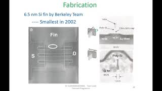
Fin quantization refers to the effect that arises in FinFET technology due to the physical structure of the device. In traditional planar transistors, one might deal with continuous dimensions, but in FinFETs, the fins are discrete structures which can lead to variability in their electrical characteristics. Therefore, it is essential to carefully size the gates (the control terminals) and loads (the connected circuits). Proper sizing ensures that the FinFET operates efficiently, avoiding potential operational errors or inefficiencies.
Examples & Analogies
Imagine you’re trying to fit various shaped blocks into a storage unit. If the blocks are too small or too large compared to the spaces available, you won’t be able to store them effectively. In a similar way, if the fins (the 'blocks') and their associated gates and loads are not sized correctly in FinFETs, the performance of the circuit will suffer.
EDA Tool Requirements
Chapter 2 of 4
🔒 Unlock Audio Chapter
Sign up and enroll to access the full audio experience
Chapter Content
● Requires FinFET-aware PDKs, design rules, and layout constraints.
Detailed Explanation
Electronic Design Automation (EDA) tools are essential for designing integrated circuits. To work efficiently with FinFETs, these tools need to be adapted specifically to accommodate the unique properties of FinFET technology. This means creating Process Design Kits (PDKs) that include rules and constraints tailored to FinFETs. Without these custom adaptations, designers may face challenges in accurately simulating, designing, and fabricating circuits that utilize FinFETs, which could lead to large-scale issues once manufacturing begins.
Examples & Analogies
Think of EDA tools as specialized chefs equipped with unique tools and recipes for different cuisines. A chef who specializes in Italian cuisine might need specific tools and ingredients not used in Japanese cuisine. Similarly, for FinFET designs, EDA tools need the right 'recipes' and parameters to create effective circuit designs, ensuring smooth operation and manufacturing.
Thermal Management Issues
Chapter 3 of 4
🔒 Unlock Audio Chapter
Sign up and enroll to access the full audio experience
Chapter Content
● High transistor density → increased local hotspots.
Detailed Explanation
As FinFET technology allows for a significantly higher density of transistors on a chip, the amount of heat generated in certain areas—known as local hotspots—also increases. Managing this heat is crucial for maintaining chip performance and reliability. If these hotspots are not adequately addressed, they could lead to overheating, which can damage the chip or cause it to malfunction. Therefore, engineers must integrate efficient thermal management solutions into their designs to disperse heat effectively.
Examples & Analogies
Consider how buildings require proper ventilation systems to avoid overheating, especially in densely populated areas. Just as homes may need fans or air conditioning to manage heat, FinFET designs need clever cooling solutions to disperse the heat produced by densely stacked transistors. Without proper ventilation in either case, significant problems can arise, be it discomfort or device failure.
Manufacturing Cost Considerations
Chapter 4 of 4
🔒 Unlock Audio Chapter
Sign up and enroll to access the full audio experience
Chapter Content
● 3D patterning and lithography increase fabrication expense.
Detailed Explanation
The advanced techniques used in FinFET manufacturing, such as 3D patterning and specialized lithography processes, result in increased fabrication expenses compared to traditional planar technology. These techniques allow for smaller, more complex structures but also require more sophisticated and costly equipment and materials. This increase in costs can impact the overall affordability of chips using FinFET technology, especially for lower-volume applications.
Examples & Analogies
Imagine a construction project that involves building a skyscraper versus a single-story home. The skyscraper requires advanced techniques, specialized labor, and expensive materials, leading to higher overall costs. Similarly, manufacturing FinFETs is akin to building the more complex skyscraper as it leverages advanced technology, resulting in increased production costs compared to simpler designs.
Key Concepts
-
Fin Quantization: Refers to the discrete nature of the fins in FinFETs affecting their electrical characteristics.
-
EDA Tools: Essential for designing and simulating circuits, specifically optimized for FinFET architectures.
-
Thermal Management: Critical in managing heat generated by high-density transistor arrangements.
-
Manufacturing Costs: Increased complexity in production due to advanced techniques required for FinFET fabrication.
Examples & Applications
In FinFET designs, if designs are not optimized for fin quantization, we may see excessive power consumption in circuits.
Advanced EDA tools can simulate thermal scenarios allowing engineers to preemptively design against hotspots.
Memory Aids
Interactive tools to help you remember key concepts
Rhymes
Fine fins must be right, or circuits won’t delight.
Stories
Once upon a time, in a land of tiny transistors, the wise engineers had to carefully size the fins. If they didn't, the kingdom's circuits faltered, and the performance of their devices fell to ruin.
Memory Tools
F.A.T. C. - Fin quantization, Advanced EDA tools, Thermal management, Cost challenges.
Acronyms
FINT - Fin quantization, Integration tools (EDA), Necessary thermal management, and True cost considerations.
Flash Cards
Glossary
- Fin Quantization
The discrete nature of FinFET fins that affects the design and functionality of transistors in integrated circuits.
- EDA
Electronic Design Automation; tools used for designing electronic systems and circuits.
- PDK
Process Design Kit; a collection of files and rules necessary for designing integrated circuits.
- Thermal Management
Techniques used to control the temperature within electronic devices to prevent overheating and ensure performance.
- Manufacturing Cost
The total expense incurred in the production of semiconductors, influenced by design complexity, materials, and equipment used.
Reference links
Supplementary resources to enhance your learning experience.