
Module 3: Week 3 - Introduction to FPGAs and Synthesis
Interactive Audio Lesson
Listen to a student-teacher conversation explaining the topic in a relatable way.
Introduction to FPGAs
🔒 Unlock Audio Lesson
Sign up and enroll to listen to this audio lesson

Today we'll explore Field-Programmable Gate Arrays or FPGAs. Can anyone tell me what makes FPGAs unique compared to traditional circuits?

Are FPGAs programmable after they are made?
Exactly! FPGAs are unique because they can be reconfigured after manufacturing. This leads to immense flexibility in design. Think of them as a blank canvas for creating custom circuits. This is often referred to as their 'field-programmable' aspect.

So, we can change how they function even after they are installed?
Correct! By loading a new configuration bitstream, we can change how an FPGA operates. This is crucial for applications that need to adapt to new standards or requirements.

Can we compare them directly with ASICs?
Yes, that's a great question! Unlike ASICs, which are custom-built for specific tasks, FPGAs allow for post-manufacturing changes. Would anyone like to summarize the differences we just discussed?

FPGAs can be altered after production, while ASICs cannot be changed once made.
Excellent summarization! FPGAs provide flexibility, reducing costs and development time for rapidly changing technologies.
Understanding FPGA Architecture
🔒 Unlock Audio Lesson
Sign up and enroll to listen to this audio lesson

Let’s move on to the internal architecture of FPGAs. Who can tell me about the core components like Configurable Logic Blocks?
Are CLBs the main processing units in FPGAs?
That's right! CLBs house Configurable Logic Arrays, allowing complex logic functions. Let's remember this with the acronym CLB - 'Central Logic Block.' Any ideas on what else might be inside?
Look-Up Tables, right?
Exactly! LUTs are essential as they define how inputs map to outputs in combinational logic. Remember, LUT can also mean 'Logic Unit Table.' Another key component is the Flip-Flop for sequential logic. Can anyone explain how these work?
They store data bits until the next clock cycle?
Correct! Flip-Flops react to clock edges and are critical for timing in circuits.
Can CLBs and LUTs work together?
Yes! CLBs utilize LUTs and Flip-Flops to implement desired logic functions. Understanding these combinations will be pivotal in synthesis later!
HDLs and Their Importance
🔒 Unlock Audio Lesson
Sign up and enroll to listen to this audio lesson
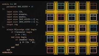
Next, let’s discuss Hardware Description Languages, or HDLs. Why do you think we need HDLs for FPGA design?
To describe how the hardware works?
Exactly! HDLs allow designers to specify behavior and structure abstractly. Think of it as writing instructions for a robot. Anyone know the two main types of HDLs?
Verilog and VHDL?
Great job! Verilog is often easier for those familiar with C, while VHDL emphasizes stricter typing and can be more verbose. Can you see how each caters to different preferences?
Yes, but what about their uses?
Both are used for synthesis and simulation of digital systems. This brings us to the synthesis process. Any idea what synthesis does?
It converts HDL descriptions into hardware designs?
Correct! Synthesis transforms HDLs into gate-level representations for specific technologies. Excellent work today!
Logic Synthesis Process
🔒 Unlock Audio Lesson
Sign up and enroll to listen to this audio lesson
Finally, let’s explore the logic synthesis process itself. What are the main steps involved?
I think it starts with parsing the HDL code?
Correct! The first step is elaboration, where the HDL is interpreted. Then comes generic logic optimization. What do we want to achieve in this phase?
To simplify logic and reduce redundancy?
Right again! This is vital to ensure efficient mapping later. After that, we perform technology mapping, where we adapt our design.
What does that mean exactly?
Technology mapping involves selecting suitable physical resources like LUTs and flip-flops. Finally, we generate a netlist, which is a detailed description of the circuit. Let’s remember that with the mnemonic 'E-G-T-N' for Elaboration, G-Logic optimization, T-Technology mapping, and N-Netlist generation.
Could you explain what a netlist is again?
Certainly! A netlist is our final output that defines how components connect. It becomes crucial for hardware implementation.
Great recap, thank you!
Introduction & Overview
Read summaries of the section's main ideas at different levels of detail.
Quick Overview
Standard
Students will explore Field-Programmable Gate Arrays (FPGAs), understanding their reconfigurable architecture, core functionalities, and the synthesis process pivotal for converting HDLs into physical hardware configurations. The module compares FPGAs with ASICs and microcontrollers, equipping students with essential knowledge for embedded systems.
Detailed
Detailed Summary
This module serves as an extensive introduction to Field-Programmable Gate Arrays (FPGAs) and the critical process of synthesis.
Key Focus Areas:
- FPGAs: Understanding their architecture, the unique advantages they offer such as reconfigurability, and how they differ from ASICs and microcontrollers is essential. The section elaborates on the components such as Configurable Logic Blocks (CLBs), programmable interconnects, and Input/Output Blocks (IOBs), showcasing how these contribute to the flexibility and efficiency of FPGAs in different applications.
- Hardware Description Languages (HDLs): Emphasis is placed on the role of HDLs, particularly Verilog and VHDL, in modeling digital systems. These languages enable designers to describe hardware functionality, leading into a detailed examination of each language, their syntax, and structured methodologies for design.
- Logic Synthesis: This process is explained in depth, describing how it bridges the gap between HDL descriptions and physical hardware. Topics include multi-stage synthesis, technology mapping, and the tuning of designs for performance metrics—speed, area, and power.
Importance of This Knowledge:
Understanding FPGAs and synthesis is crucial for students looking to build advanced, high-performance embedded systems. This module elucidates how design iterations can be rapidly implemented, enabling innovation and efficient prototyping.
Youtube Videos


Audio Book
Dive deep into the subject with an immersive audiobook experience.
Module Objective Overview
Chapter 1 of 10
🔒 Unlock Audio Chapter
Sign up and enroll to access the full audio experience
Chapter Content
Upon the successful completion of this extensively detailed module, students will possess a profound, hands-on-ready understanding of Field-Programmable Gate Arrays (FPGAs) as a dynamically reconfigurable hardware platform critical for modern embedded system implementations.
Detailed Explanation
This section outlines the primary goal of the module, which is to equip students with both theoretical knowledge and practical experience concerning FPGAs. It emphasizes the importance of understanding how FPGAs work as reconfigurable hardware, which allows developers to alter the functionality of the hardware even after it has been manufactured.
Examples & Analogies
Imagine an artist with a canvas that can be repainted however they like. Similar to how they can express different ideas with colors and brushes, an FPGA allows engineers to design various electronic circuits that can adapt to different needs without creating a completely new physical chip.
Understanding FPGAs
Chapter 2 of 10
🔒 Unlock Audio Chapter
Sign up and enroll to access the full audio experience
Chapter Content
This foundational section provides an exhaustive understanding of FPGAs, their operational principles, architectural nuances, and their strategic positioning within the vast landscape of embedded hardware solutions.
Detailed Explanation
This chunk introduces FPGAs as versatile devices that allow users to reconfigure their internal architecture after production. It explains the critical role FPGAs play in modern technology, especially in applications where hardware flexibility is vital. It also emphasizes the distinctiveness of FPGAs compared to traditional fixed-function chips, enhancing their appeal in various applications.
Examples & Analogies
Think of FPGAs like a Swiss Army knife, which has multiple tools within it. Each tool can be adjusted or folded out depending on the need—just like every part of an FPGA can be configured for different tasks, making it as useful as possible in different scenarios.
Definitive Concept and Fundamental Principles of FPGAs
Chapter 3 of 10
🔒 Unlock Audio Chapter
Sign up and enroll to access the full audio experience
Chapter Content
A Field-Programmable Gate Array (FPGA) stands as a unique class of semiconductor device that distinguishes itself through its post-manufacturing reconfigurability...
Detailed Explanation
FPGAs are unique in that they can be reconfigured by the user after manufacturing, which is a significant advantage over Application-Specific Integrated Circuits (ASICs) that have fixed functions. The user can upload configuration files to change the function of the FPGA, allowing for considerable flexibility in digital designs.
Examples & Analogies
Consider a smartphone that can update its software to add new features or applications. Similarly, an FPGA can be updated or reprogrammed to perform different tasks, enhancing its usability and lifespan.
Digital Canvas Analogy
Chapter 4 of 10
🔒 Unlock Audio Chapter
Sign up and enroll to access the full audio experience
Chapter Content
Consider an FPGA as a highly versatile, digital 'blank canvas' or a three-dimensional, reconfigurable electronic breadboard...
Detailed Explanation
This analogy highlights how an FPGA functions as a customizable platform. Just as an artist can create unique images on a blank canvas, engineers can use their creativity to design various digital circuits on an FPGA. The ability to load different configurations allows for experimentation and innovation in design.
Examples & Analogies
An FPGA can be likened to a LEGO set where you can build different structures with the same blocks over and over. Each design can be taken apart and reassembled to create something new, which mirrors the reconfigurable nature of FPGAs.
Deep Dive into FPGA's Internal Architecture
Chapter 5 of 10
🔒 Unlock Audio Chapter
Sign up and enroll to access the full audio experience
Chapter Content
To fully appreciate the power of FPGAs, a detailed understanding of their internal composition is crucial...
Detailed Explanation
This part of the module outlines the essential components that make up an FPGA, including Configurable Logic Blocks (CLBs), programmable interconnects, Input/Output Blocks (IOBs), and specialized Hard IP blocks. These internal elements work together to enable the functional versatility of FPGAs.
Examples & Analogies
Think of an FPGA's architecture like the various parts of a computer: the CPU (like CLBs), memory (like BRAM), and communication ports (like IOBs) all work together to process and manage information. Each part has its specific function, and all must work harmoniously for the system to perform effectively.
Core Concepts: Configurable Logic Blocks (CLBs)
Chapter 6 of 10
🔒 Unlock Audio Chapter
Sign up and enroll to access the full audio experience
Chapter Content
...These are the primary computational and storage units of an FPGA, typically arranged in a two-dimensional grid...
Detailed Explanation
CLBs are the heart of FPGAs, enabling them to perform various logic operations. Each block can adapt based on the user's design requirements, which is essential for creating complex digital circuits. They contain Look-Up Tables (LUTs), which enable them to implement any logical function.
Examples & Analogies
Imagine CLBs as a set of building blocks. Depending on how you arrange them, you can create a house, a car, or any structure you imagine. Each arrangement allows for different functionalities, just as CLBs can be configured for different logical operations.
Understanding Look-Up Tables (LUTs) and their Functionality
Chapter 7 of 10
🔒 Unlock Audio Chapter
Sign up and enroll to access the full audio experience
Chapter Content
At the core of each CLB's combinational logic is one or more Look-Up Tables (LUTs)...
Detailed Explanation
LUTs allow FPGAs to efficiently implement any boolean function. By storing truth tables in memory, they can provide outputs based on specific input combinations, making them fundamental in processing digital logic. LUTs are crucial for enabling the FPGA to realize complex functionalities without needing many discrete components.
Examples & Analogies
Think of a LUT like a recipe book in a kitchen. When someone wants to make a dish, they refer to the recipe, which outlines the ingredients based on the desired outcome. Similarly, LUTs store outputs based on the combinations of inputs they receive, providing quick and efficient access to necessary calculations.
Programmable Interconnects/Routing Resources
Chapter 8 of 10
🔒 Unlock Audio Chapter
Sign up and enroll to access the full audio experience
Chapter Content
This is the vast and flexible network of wires and programmable switches that enable all the individual logic blocks (CLBs/LABs)...
Detailed Explanation
Routing resources within an FPGA connect various components, allowing signals to travel across the chip to execute complex tasks. The efficiency of these interconnections plays a critical role in determining the overall performance of the FPGA, as longer or more complicated routes can introduce delays.
Examples & Analogies
The programmable interconnects can be compared to roads in a city. Just as roads allow cars to navigate from one place to another, these interconnects facilitate the travel of signals within an FPGA, ensuring they reach their destinations quickly and efficiently.
Input/Output Blocks (IOBs)
Chapter 9 of 10
🔒 Unlock Audio Chapter
Sign up and enroll to access the full audio experience
Chapter Content
These blocks are strategically located at the periphery of the FPGA die, forming the critical interface between the FPGA's internal logic and the external pins of the physical package...
Detailed Explanation
IOBs are critical connections between the FPGA and the outside world, enabling communication with other devices. These blocks are programmable to comply with various voltage and signaling standards, making FPGAs adaptable for interfacing with numerous external components.
Examples & Analogies
IOBs can be visualized as the ports on a computer that allow it to connect with other peripherals, like USB drives or monitors. Just as these ports facilitate interaction with the outside world, IOBs ensure FPGAs communicate effectively with other electronic systems.
Specialized Hard IP Blocks
Chapter 10 of 10
🔒 Unlock Audio Chapter
Sign up and enroll to access the full audio experience
Chapter Content
Modern FPGAs are no longer just arrays of generic logic...
Detailed Explanation
Hard IP blocks enhance the capability of FPGAs by providing pre-designed, optimized circuits for specific tasks, such as Digital Signal Processing (DSP) or memory management. These blocks improve performance and efficiency by handling tasks faster and using less power than generic logic.
Examples & Analogies
Think of these hard IP blocks as specialized tools in a toolbox. Just like scissors can cut paper more efficiently than using a general-purpose knife, these blocks perform specialized tasks that increase the FPGA's overall effectiveness and efficiency in applications.
Key Concepts
-
FPGAs allow post-manufacturing reconfiguration, providing flexibility.
-
CLBs house essential elements like LUTs and Flip-Flops enabling versatile logic designs.
-
HDLs, especially Verilog and VHDL, are crucial for describing hardware in an abstract manner.
-
Logic synthesis translates HDLs into optimized hardware representations, crucial for implementing designs.
Examples & Applications
An FPGA can be configured to implement a digital filter by loading a specific configuration bitstream.
A 6-input LUT can create any 6-input Boolean function, unlike fixed gates.
Memory Aids
Interactive tools to help you remember key concepts
Rhymes
FPGAs are flexible and grand, reprogramming circuits right in hand.
Stories
Imagine a LEGO set that can be rebuilt every time you want something new — that's how an FPGA functions, adapting to different tasks and designs as needed.
Memory Tools
To remember synthesis phases, use 'E-L-T-N': Elaboration, Logic optimization, Technology mapping, Netlist generation.
Acronyms
CLB - 'Central Logic Block' helps remember the key component in FPGAs.
Flash Cards
Glossary
- FPGA
Field-Programmable Gate Array; a semiconductor device that can be reprogrammed after manufacturing.
- CLB
Configurable Logic Block; the fundamental unit within an FPGA that contains LUTs and Flip-Flops.
- LUT
Look-Up Table; a digital memory used to implement logic functions.
- FlipFlop
A basic memory element that stores a single bit of data, dependent on clock signal transitions.
- HDL
Hardware Description Language; a specialized language for describing the behavior and structure of electronic systems.
- Synthesis
The process of translating HDL descriptions into a technology-specific gate-level netlist.
- Netlist
A representation of the electronic circuit that defines how various components are connected.
Reference links
Supplementary resources to enhance your learning experience.