
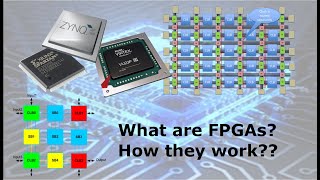
Components of FPGA Architecture
Enroll to start learning
You’ve not yet enrolled in this course. Please enroll for free to listen to audio lessons, classroom podcasts and take practice test.
Interactive Audio Lesson
Listen to a student-teacher conversation explaining the topic in a relatable way.
Logic Blocks
🔒 Unlock Audio Lesson
Sign up and enroll to listen to this audio lesson

Today, we will discuss one of the core components of FPGAs - Logic Blocks. Who can tell me what logic blocks are used for in FPGAs?

Are they the ones that perform logical operations, like AND and OR?
Exactly! Logic blocks contain Look-Up Tables, or LUTs, which perform combinatorial logic, and flip-flops that store data. Can anyone remember what a LUT does?

It looks up the values for logical functions, right?
Correct! So remember, LUT stands for Look-Up Table. Let’s move on to why flexibility in programming these blocks is beneficial — how does customizing logic help in design?

It allows engineers to adapt their design to specific needs without creating new hardware!
Excellent point! Customizability is key in FPGA design. To remember this, think of L-U-T only enables flex from your design, leading to unique functionalities.
Routing
🔒 Unlock Audio Lesson
Sign up and enroll to listen to this audio lesson

Next up, let’s dive into the routing fabric of FPGAs. Can someone explain what routing is in the context of FPGAs?

It connects the logic blocks and lets them communicate with each other, right?
Correct! The routing fabric consists of a network of wires that is also programmable. Why might this programmability be important?
It allows for flexible signal connections based on the design requirements.
Exactly! Flexible connections = better performance in specific applications. Think of it as a smart road system where the paths can change dynamically for better traffic flow.
That’s a cool analogy! It makes it easier to remember.
I/O Blocks
🔒 Unlock Audio Lesson
Sign up and enroll to listen to this audio lesson
Let’s discuss I/O blocks — Who can tell me their role in FPGA architecture?
They manage the input and output signals between the FPGA and other devices.
Great job! These blocks are essential for facilitating communication. What kinds of applications might require high-speed I/O?
Maybe something like video processing or real-time systems?
Exactly! I/O blocks ensure that FPGAs can effectively interact in systems like those. Remember, high-speed communication is vital in applications requiring quick data exchange.
Configuration Memory
🔒 Unlock Audio Lesson
Sign up and enroll to listen to this audio lesson
Now, let’s move to configuration memory. What is its primary function?
It stores the bitstream that determines how the FPGA behaves.
Right! And this capability of being reprogrammed makes FPGAs extremely versatile. Why do you think this aspect is significant?
Because it means you can change its function without changing the actual hardware!
Exactly! Modern applications often change demands, which makes reprogrammability a major advantage of FPGAs. Just think of configuration memory as the 'brain' of the FPGA that can forget and learn new tasks!
Summary of FPGA Components
🔒 Unlock Audio Lesson
Sign up and enroll to listen to this audio lesson
Alright, let’s summarize what we learned today about FPGA components. Someone give me the main components we discussed.
Logic blocks, routing, I/O blocks, and configuration memory.
Great! Can anyone explain how these components work together to provide flexibility?
They all allow for custom logic design and adaptability, which means engineers can create tailored solutions efficiently.
Absolutely! Remember these components and how they interact, as they're the building blocks to understanding FPGA functionality. You can think of these as a team working together to solve problems!
Introduction & Overview
Read summaries of the section's main ideas at different levels of detail.
Quick Overview
Standard
An exploration of the fundamental components of FPGA architecture is presented, highlighting how logic blocks, routing fabric, I/O blocks, and configuration memory collectively enable the customization and flexibility of FPGAs for various applications.
Detailed
Components of FPGA Architecture
FPGAs, or Field-Programmable Gate Arrays, are comprised of several critical components that contribute to their versatile nature. These components include:
Logic Blocks
Logic blocks are the fundamental building elements of FPGAs. They include:
- Look-Up Tables (LUTs): Perform combinatorial logic functions.
- Flip-Flops: Store data temporarily.
These blocks are highly programmable, allowing for tailored implementations of logic functions depending on the system's requirements.
Routing
The routing fabric connects all logic blocks within the FPGA. It features a complex network of programmable wires that facilitates the flexible transfer of signals between blocks, significantly enhancing interconnectivity.
I/O Blocks
I/O blocks function as the interface between the FPGA and other external devices. They are crucial in handling input and output signals, supporting high-speed communications necessary for efficient operation.
Configuration Memory
This component stores the bitstream that defines the FPGA's behavior. Since the configuration memory can be reprogrammed, FPGAs possess the adaptability to fulfill various functions and applications, providing flexibility in design without requiring hardware changes.
Understanding these components is essential as they underscore how FPGAs can be programmed to meet changing requirements and contribute to the development of complex digital systems.
Youtube Videos


Audio Book
Dive deep into the subject with an immersive audiobook experience.
Logic Blocks
Chapter 1 of 4
🔒 Unlock Audio Chapter
Sign up and enroll to access the full audio experience
Chapter Content
● Logic Blocks:
○ These are the basic building blocks that implement the logic functions. They contain Look-Up Tables (LUTs), which perform combinatorial logic, and flip-flops that store data.
○ Logic blocks are highly programmable, allowing designers to implement custom logic based on their specific needs.
Detailed Explanation
Logic blocks are fundamental units within FPGA architecture. Each logic block contains:
1. Look-Up Tables (LUTs): These can perform various logical operations by storing truth values. They enable the logic block to execute complex functions based on the inputs.
2. Flip-Flops: These are used for storing bits of information, essentially acting as memory elements to hold data temporarily.
Because they are programmable, designers can customize these blocks to create unique logic circuits tailored specifically to their application requirements.
Examples & Analogies
Think of logic blocks like a set of building blocks for a toy house. Each block can represent a different function or feature of the house. Just as children can mix and match these blocks to design their dream house, engineers can configure logic blocks in an FPGA to build digital circuits that meet specific needs.
Routing
Chapter 2 of 4
🔒 Unlock Audio Chapter
Sign up and enroll to access the full audio experience
Chapter Content
● Routing:
○ The routing fabric connects the logic blocks and allows signals to travel between them. It consists of a complex network of wires that are also programmable, enabling flexible interconnection between different parts of the FPGA.
Detailed Explanation
The routing component of an FPGA acts as the communication pathway between logic blocks. Here's how it works:
- Interconnection: The routing fabric is a network of programmable wires that can connect any two logic blocks.
- Flexibility: Since these routes are programmable, designers can change the way components interact without needing new hardware, allowing adjustments to be made based on performance needs or design changes.
Examples & Analogies
Imagine routing in an FPGA like a city's road system. Just as roads connect houses (logic blocks), the routing allows different blocks to communicate. In a city, you can redesign the layout to improve traffic flow; similarly, in an FPGA, you can reconfigure the routing to create the most efficient design for data transfer.
I/O Blocks
Chapter 3 of 4
🔒 Unlock Audio Chapter
Sign up and enroll to access the full audio experience
Chapter Content
● I/O Blocks:
○ These blocks manage the interface between the FPGA and external devices. They provide high-speed communication capabilities for input and output signals.
Detailed Explanation
I/O blocks are crucial for connecting the FPGA to the outside world. They serve the following roles:
- Input/Output Management: They handle signals coming into and going out from the FPGA. This means data can be received and sent to other devices like sensors, processors, or communication interfaces.
- High-Speed Communication: I/O blocks are designed for fast communication, ensuring that data transfer between the FPGA and external devices is efficient and timely.
Examples & Analogies
Consider I/O blocks as the doors and windows of a house. They allow people (data) to move in and out easily while maintaining security and speed. Just as doors can be designed for efficiency, I/O blocks ensure seamless communication with the world outside the FPGA.
Configuration Memory
Chapter 4 of 4
🔒 Unlock Audio Chapter
Sign up and enroll to access the full audio experience
Chapter Content
● Configuration Memory:
○ The configuration memory stores the FPGA's bitstream (the program that defines its behavior). This memory can be reprogrammed, making FPGAs adaptable to different functions and applications.
Detailed Explanation
Configuration memory is essential for the functionality of an FPGA because it determines how the device behaves. Key points include:
- Storing Bitstream: The bitstream is the set of instructions that configures the FPGA’s logic blocks, routing, and I/O behavior.
- Reprogrammable Nature: Unlike traditional chips, which have fixed functions, the configuration memory allows the FPGA to be reprogrammed for different tasks or projects, enhancing its versatility.
Examples & Analogies
Think of configuration memory like the blueprint for a building. Before construction begins, architects use blueprints to determine how everything will fit together; similarly, the bitstream configures the FPGA to behave in a specific way. After construction, if the building needs to serve a new purpose, you can change the blueprint for modifications, much like reprogramming the FPGA.
Key Concepts
-
Logic Blocks: Fundamental components in FPGAs for implementing logic functions.
-
Routing: The interconnection network in FPGAs that allows signals to be routed between logic blocks.
-
I/O Blocks: Interfaces of the FPGA that handle communication with external devices.
-
Configuration Memory: Memory responsible for storing the bitstream that defines the FPGA's behavior, allowing reconfiguration.
Examples & Applications
Example of a Logic Block: A simple combination of a LUT and flip-flops could be used to create a counter circuit.
Example of Routing: In a communication application, routing enables simultaneous data transfer between multiple logic blocks to enhance processing speed.
Memory Aids
Interactive tools to help you remember key concepts
Rhymes
Logic blocks work with a table to hop, / To form logic, and never stop!
Stories
Imagine an FPGA as a bustling city: Logic Blocks are houses where computations occur, Routing is the road network connecting them, I/O Blocks are highways to the outside world, and Configuration Memory is the city planner, always ready to redesign the layout!
Memory Tools
Remember 'L-R-I-C' for the FPGA components: Logic Blocks, Routing, I/O Blocks, Configuration Memory.
Acronyms
Use 'LIRMC' as an acronym — Logic, I/O, Routing, Memory Configuration.
Flash Cards
Glossary
- Logic Blocks
The basic building blocks of FPGAs, including Look-Up Tables (LUTs) and flip-flops, used to implement logic functions.
- LookUp Table (LUT)
A memory structure used in digital circuits to implement combinatorial logic, allowing the FPGA to perform specific logical operations.
- Routing
The network of programmable wires that interconnects different logic blocks within an FPGA.
- I/O Blocks
Blocks that manage the interfaces for input and output signals between the FPGA and external devices.
- Configuration Memory
Memory within an FPGA that stores the bitstream, which defines its operational behavior and can be reprogrammed.
Reference links
Supplementary resources to enhance your learning experience.