
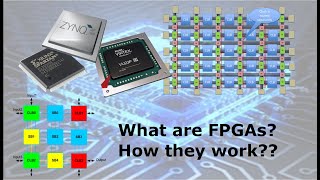
Design Flow for FPGA Programming
Enroll to start learning
You’ve not yet enrolled in this course. Please enroll for free to listen to audio lessons, classroom podcasts and take practice test.
Interactive Audio Lesson
Listen to a student-teacher conversation explaining the topic in a relatable way.
Design Entry
🔒 Unlock Audio Lesson
Sign up and enroll to listen to this audio lesson

Alright class, let's begin with the first stage of our design flow: Design Entry. This is where we write our HDL code to define the FPGA's behavior. Can anyone tell me what HDL stands for?

Is it Hardware Description Language?
Exactly! We typically use languages like VHDL or Verilog. Remember, VHDL emphasizes readability, while Verilog's syntax resembles C, which can make it easier for those familiar with software programming. What might be some advantages of using HDL?

HDLs allow for high-level abstraction, making design modifications easier.
Great point! This abstraction is crucial for efficient design entry. To help remember this concept, think of HDL as your blueprint for a house. What happens if we want to change the floor plan after construction?

We would need to tear down parts of the house!
Exactly—modifying hardware is much more complex than changing the HDL code itself. Let's summarize this step: Design Entry is the groundwork for our project, utilizing HDL for defining the desired behavior.
Synthesis
🔒 Unlock Audio Lesson
Sign up and enroll to listen to this audio lesson

Moving on to the second step: Synthesis. Can anyone explain what this phase entails?
It transforms the HDL code into a netlist, which describes how components are interlinked.
Exactly! A netlist is crucial because it translates our abstract design into something tangible. Think of it as the instructions for building a puzzle. What do you think happens if the synthesis process does not succeed?

We might have errors in our design that could lead to a malfunction?
Right! An unsuccessful synthesis could mean our design needs further refinement. Always check for synthesis warnings! Now, to remember synthesis, think of it as the moment we take our cake recipe and turn it into an actual cake.
Implementation
🔒 Unlock Audio Lesson
Sign up and enroll to listen to this audio lesson
Now let's discuss Implementation. What do we accomplish in this stage?
We map the netlist onto the actual FPGA architecture!
Exactly! Implementation involves allocating logic blocks and routing resources. Can anyone tell me why optimization is important during this phase?
It improves performance and saves resources!
Correct! Optimization can lead to better efficiency in power usage and speed. Think of this phase like organizing a toolbox—everything must be in its place for efficiency!
Bitstream Generation
🔒 Unlock Audio Lesson
Sign up and enroll to listen to this audio lesson
The next step is Bitstream Generation. What do we mean by 'bitstream'?
It's the file containing all the instructions for the FPGA configuration!
Great! The bitstream is crucial; it essentially tells the FPGA how to function. Why do you think this process is pivotal in FPGA programming?
Without the bitstream, the FPGA wouldn't know how to carry out the programmed design!
Exactly! It encapsulates our design and dictates the configuration. Remember, the bitstream is like the final version of our recipe, full of instructions for baking the cake!
Programming the FPGA
🔒 Unlock Audio Lesson
Sign up and enroll to listen to this audio lesson
Finally, we reach the Programming stage. What does this involve?
We upload the generated bitstream to the FPGA using a programmer or JTAG!
That's right! This action brings our design to life within the FPGA hardware. Now, if the programming step fails, what might that indicate?
There could be errors in the bitstream or issues with the programming hardware?
Correct! Any errors here must be resolved. To remember this final step, think of it as the moment you turn on the oven for your cake. It’s where everything you've worked on comes to fruition. Let’s summarize: The Programming phase is the culmination of our design process.
Introduction & Overview
Read summaries of the section's main ideas at different levels of detail.
Quick Overview
Standard
The design flow for FPGA programming includes several key stages, starting from design entry with HDL code, through synthesis and implementation, to generating a configuration bitstream that is ultimately used to program the FPGA.
Detailed
Design Flow for FPGA Programming
In this section, we delve into the detailed design flow required for programming Field-Programmable Gate Arrays (FPGAs). This modular approach not only enhances understanding but also ensures that designers can effectively utilize FPGAs for various applications. The design flow consists of several critical steps:
- Design Entry: Initially, the designer writes the FPGA code using Hardware Description Languages (HDLs) like VHDL or Verilog, employing tools such as Xilinx Vivado or Intel Quartus to facilitate this process.
- Synthesis: The next phase involves synthesizing the HDL code into a netlist. This netlist defines the logical connections among the various components of the design, aligning the high-level description to a representation suitable for implementation.
- Implementation: During this phase, the netlist is mapped onto the FPGA's architecture. This involves allocating the required logic blocks and routing resources to ensure that the design functions as intended within the FPGA.
- Bitstream Generation: After successful implementation, the configuration bitstream is generated. This bitstream contains all the necessary instructions that define how the FPGA should behave.
- Programming: The final step is programming the FPGA with the generated bitstream, which can be accomplished using external hardware programmers or through JTAG connections.
This structured design flow is significant as it allows for systematic development, debugging, and optimization of FPGA applications, making them adaptable and efficient.
Youtube Videos


Audio Book
Dive deep into the subject with an immersive audiobook experience.
Design Entry
Chapter 1 of 5
🔒 Unlock Audio Chapter
Sign up and enroll to access the full audio experience
Chapter Content
The designer writes the HDL code for the FPGA using tools such as Xilinx Vivado or Intel Quartus.
Detailed Explanation
In the first step of the design flow, the designer creates the Hardware Description Language (HDL) code, which provides the specifications for what the FPGA should do. This code can include the logic that will be implemented on the FPGA and is written in either VHDL or Verilog. Designers use specialized software tools like Xilinx Vivado or Intel Quartus to aid in coding and manage the design process efficiently.
Examples & Analogies
Think of this step like writing a recipe for a dish. Just as you write down ingredients and instructions before cooking, a designer must outline the necessary logic and operations in code before the FPGA can perform tasks.
Synthesis
Chapter 2 of 5
🔒 Unlock Audio Chapter
Sign up and enroll to access the full audio experience
Chapter Content
The HDL code is synthesized to generate a netlist, which describes the logical interconnections between components.
Detailed Explanation
In the synthesis stage, the HDL code is processed by the synthesis tool to create a netlist. A netlist is essentially a blueprint that outlines how various components in the design are interconnected logically. It transforms the high-level description of the design into a format that reflects the actual hardware components used in the FPGA, ensuring everything is correctly linked according to the design specifications.
Examples & Analogies
This step can be likened to an architect providing detailed plans based on a blueprint. The synthesis translates the abstract design (HDL code) into concrete connections and components that will be used to physically create the structure (the FPGA's functionality).
Implementation
Chapter 3 of 5
🔒 Unlock Audio Chapter
Sign up and enroll to access the full audio experience
Chapter Content
The netlist is mapped onto the FPGA architecture, with logic blocks and routing resources allocated accordingly.
Detailed Explanation
During the implementation phase, the netlist generated from synthesis is mapped to the physical resources available on the FPGA. This involves allocating specific logic blocks to specific functions and determining how signals will be routed between those blocks. The tool optimizes these allocations to ensure the design works efficiently within the FPGA's architecture.
Examples & Analogies
Consider this step as arranging furniture in a room based on the available space. Just like choosing where to place a sofa or table based on the room's layout, this step ensures the logical functions fit into the FPGA's architecture and work seamlessly together.
Bitstream Generation
Chapter 4 of 5
🔒 Unlock Audio Chapter
Sign up and enroll to access the full audio experience
Chapter Content
The configuration bitstream is generated, which contains the information required to configure the FPGA.
Detailed Explanation
When the implementation is complete, a configuration bitstream is generated. This bitstream is a file that contains all the necessary data needed to configure the FPGA's hardware based on the netlist. It defines how the FPGA should be set up to execute the design described in the HDL code, including how to connect various components and manage their functionality.
Examples & Analogies
Think of the bitstream as the set-up instructions for a new video game. Just as the game needs specific data to operate (like levels, characters, and rules), the FPGA requires the configuration data in the bitstream to know how to function according to the designer's specifications.
Programming
Chapter 5 of 5
🔒 Unlock Audio Chapter
Sign up and enroll to access the full audio experience
Chapter Content
The FPGA is programmed with the bitstream, either through a hardware programmer or via JTAG.
Detailed Explanation
In the final step, the FPGA is programmed with the previously generated bitstream. This can be done through various methods such as a hardware programmer (a device specifically designed for programming FPGAs) or using JTAG (Joint Test Action Group) interfaces, which allows for in-system programming. Once programmed, the FPGA can begin executing the design as per the configurations specified in the bitstream.
Examples & Analogies
This step can be compared to uploading software on a new smartphone. Just as you download an operating system and apps onto your phone to customize it for your needs, programming the FPGA transfers the configuration data to customize it for specific tasks.
Key Concepts
-
Design Entry: The phase where HDL code is created.
-
Synthesis: The process of converting HDL into a netlist.
-
Netlist: A description of component interconnections.
-
Implementation: Allocating resources based on the netlist.
-
Bitstream: Configuration information for the FPGA.
-
Programming: The step of loading the bitstream onto the FPGA.
Examples & Applications
For Design Entry, using Xilinx Vivado to write a simple state machine in VHDL.
During Synthesis, a designer might encounter warnings if the HDL code has syntax errors, highlighting the need for correction.
Memory Aids
Interactive tools to help you remember key concepts
Rhymes
Before we implement, design must be grand, syntax correct, our logic planned.
Stories
Imagine you are building a LEGO castle. You first sketch it out, gather pieces (Design Entry), then sort them (Synthesis), followed by constructing the base (Implementation), and finally decorating it with special flags (Programming, or Bitstream).
Memory Tools
D-S-I-B-P: Design, Synthesis, Implementation, Bitstream, Programming.
Acronyms
Use the acronym 'DSPB' to remember
Design
Synthesis
Programming
Bitstream!
Flash Cards
Glossary
- Design Entry
The first step in the FPGA design flow where the designer writes HDL code.
- Synthesis
The process of transforming HDL code into a netlist describing the logical connections.
- Netlist
A representation of the logical interconnections between components of an FPGA design.
- Implementation
The phase where the netlist is mapped onto FPGA architecture and resources are allocated.
- Bitstream
A configuration file generated from the design that tells the FPGA how to behave.
- Programming
The process of uploading the bitstream to the FPGA, finalizing the configuration.
Reference links
Supplementary resources to enhance your learning experience.