
Fabrication and Nanolithography Techniques
Enroll to start learning
You’ve not yet enrolled in this course. Please enroll for free to listen to audio lessons, classroom podcasts and take practice test.
Interactive Audio Lesson
Listen to a student-teacher conversation explaining the topic in a relatable way.
Introduction to Nanolithography
🔒 Unlock Audio Lesson
Sign up and enroll to listen to this audio lesson

Today we'll explore what nanolithography is! It's an important process in nanofabrication that allows us to create structures at the nanometer scale. Can anyone tell me why this is useful?

I think it’s used in electronics, right?
Exactly! It's essential in making integrated circuits and nanodevices. Remember, we can think of nanolithography as the building blocks for future technology. An easy way to remember this could be a rhyme: 'Small patterns, big dreams!'

But what makes it so challenging?
Great question! We often face issues like controlling defects and achieving high resolution. Think of it like drawing tiny pictures that must be perfect - any imperfection can ruin the whole piece!
Photolithography
🔒 Unlock Audio Lesson
Sign up and enroll to listen to this audio lesson

Now, let’s dive into photolithography. Can anyone describe what it involves?

It uses UV light and a photoresist, right?
Exactly! It's how most semiconductors are made. Remember the acronym 'PHOTOs' - for Photolithography Of High Throughput Semiconductors. What do you think is a limitation of this method?

The resolution is limited by the light's wavelength?
Yes! And that makes it difficult to create extremely tiny features. Keep that in mind as we contrast it with other methods.
Electron-Beam Lithography (EBL)
🔒 Unlock Audio Lesson
Sign up and enroll to listen to this audio lesson
Let’s discuss EBL. Can someone summarize its main advantage?
It can create features smaller than 10 nm.
Correct! And remember, since it uses electron beams, there's no need for physical masks - that's very flexible. However, it is quite slow. How do you think this affects its use in industry?
It wouldn't be used for mass production, I guess.
Exactly! Speed is crucial for mass production lines. It’s like a great artist – amazing detail but too slow to produce a painting for everyone.
Nanoimprint Lithography (NIL)
🔒 Unlock Audio Lesson
Sign up and enroll to listen to this audio lesson
Now, what can you tell me about NIL?
It uses a mold to create patterns, right?
Yes! It’s a physical process. A helpful way to remember this is by thinking: 'Print it like a cookie!' What’s one challenge associated with NIL?
If the mold isn’t perfect, it could mess up the pattern.
Exactly! Precision in mold fabrication is a must. Otherwise, you can have unsuccessful prints.
Dip-Pen Nanolithography (DPN)
🔒 Unlock Audio Lesson
Sign up and enroll to listen to this audio lesson
Let’s wrap up with DPN. How is it different from other techniques?
It uses an AFM tip to deposit ink on the surface.
Well done! DPN allows high precision. Remember the acronym 'DPP' - for Dip-Pen Precision. What do you think are its limitations?
It has low throughput, so not many patterns in a short time?
Exactly! Also, temperature and humidity control are crucial. Think of it like painting in a humid room – it might not dry correctly!
Introduction & Overview
Read summaries of the section's main ideas at different levels of detail.
Quick Overview
Standard
The section covers various nanolithography techniques, explaining their principles, advantages, and limitations. It emphasizes the significance of these methods in creating nanoscale structures and devices across multiple fields.
Detailed
Fabrication and Nanolithography Techniques
Nanolithography is a critical process in nanofabrication that allows creating intricate patterns on materials at the nanometer scale. This chapter elaborates on several key lithographic techniques, namely photolithography, electron-beam lithography, nanoimprint lithography, and dip-pen nanolithography.
7.1 Introduction to Nanolithography
This section introduces nanolithography as a fundamental technique for fabricating structures used in electronics and biomedical applications. It aims for high-resolution patterning with accuracy and cost-effectiveness, requiring advanced equipment and cleanroom conditions.
7.2 Photolithography
This widely used technique in semiconductor manufacturing utilizes UV light to create patterns on photoresist materials. The advantages include high throughput and scalability, while the limitations include dependency on light wavelength and complex optics.
7.3 Electron-Beam Lithography (EBL)
EBL uses a focused electron beam for patterning with a resolution below 10 nm, allowing for flexibility in design without physical masks. However, it is slow and expensive, making it unsuitable for mass production.
7.4 Nanoimprint Lithography (NIL)
NIL employs mechanical deformation of a resist using patterned molds, achieving high-resolution patterns cost-effectively. Challenges include the precision required for mold fabrication and contamination risks.
7.5 Dip-Pen Nanolithography (DPN)
DPN utilizes an AFM tip to deposit molecular ink precisely, offering high control, especially for soft materials. However, low throughput and strict environmental conditions pose challenges.
7.6 Challenges in Nanoscale Patterning
Key challenges in nanolithography include resolution limitations, overlay accuracy, defect control, material compatibility, and the cost of complex setups.
7.7 Summary
Nanolithography remains essential in the march toward smaller, high-performance devices in various fields as technological innovations continue to evolve.
Youtube Videos
Audio Book
Dive deep into the subject with an immersive audiobook experience.
Introduction to Nanolithography
Chapter 1 of 6
🔒 Unlock Audio Chapter
Sign up and enroll to access the full audio experience
Chapter Content
Nanolithography is the process of patterning materials at the nanometer scale. It is a fundamental technique in nanofabrication, enabling the creation of structures and devices used in electronics, photonics, biomedical applications, and more. Nanolithography is essential for manufacturing integrated circuits, MEMS (Microelectromechanical Systems), and nanosensors.
The goal of nanolithography is to achieve high-resolution patterning with accuracy, reproducibility, and cost-effectiveness. It often requires a combination of advanced equipment, cleanroom conditions, and precise material control.
Detailed Explanation
Nanolithography refers to techniques used to create very small patterns, typically on the scale of nanometers (one billionth of a meter). This process is crucial in nanofabrication, where it helps create tiny structures found in advanced electronics and medical devices. The primary aim is to produce intricate designs with high accuracy and reproducibility while keeping costs manageable. To successfully perform nanolithography, specialized tools, clean and controlled environments, and specific materials must be utilized.
Examples & Analogies
Think of nanolithography like using a highly precise paintbrush to create tiny, detailed artwork on a canvas. Just as an artist needs the right tools and environment to produce a masterpiece, nanolithography requires advanced equipment and controlled settings to build the tiny structures that power modern technology.
Photolithography
Chapter 2 of 6
🔒 Unlock Audio Chapter
Sign up and enroll to access the full audio experience
Chapter Content
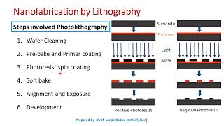
Photolithography is the most widely used lithographic method in semiconductor manufacturing. It uses ultraviolet (UV) light to transfer patterns from a mask onto a light-sensitive photoresist layer.
Working Principle:
1. A wafer is coated with a photoresist material.
2. UV light is passed through a patterned mask.
3. The exposed areas of the photoresist undergo chemical changes.
4. The wafer is developed, washing away either the exposed or unexposed regions (depending on whether a positive or negative resist is used).
Advantages:
● High throughput and scalability.
● Well-established process in industry.
Limitations:
● Resolution is limited by the wavelength of light.
● Requires complex optics and cleanroom conditions.
Detailed Explanation
Photolithography is a dominant technique in the semiconductor industry, known for its efficiency in transferring designs onto materials. The process starts by coating a material, known as a wafer, with a layer that is sensitive to light. When exposed to UV light through a mask with a pattern, the photoresist reacts chemically. After exposure, the wafer is developed, which removes either the exposed or unexposed parts, revealing the desired design. This method is widely used because it can produce high volumes of products quickly and is well-understood in the industry. However, it has limitations, such as the maximum detail size it can achieve being constrained by the properties of light.
Examples & Analogies
Imagine using a stencil to paint a design on a wall. The stencil allows you to quickly create a pattern by spraying paint over it. Similar to how the stencil requires specific dimensions to work well, photolithography depends on the wavelength of light to define how small we can make our designs. If the stencil (or light) is not fine enough, you won't get the sharp details you want.
Electron-Beam Lithography (EBL)
Chapter 3 of 6
🔒 Unlock Audio Chapter
Sign up and enroll to access the full audio experience
Chapter Content
EBL is a high-resolution lithography method that uses a focused beam of electrons to write patterns directly onto an electron-sensitive resist.
Working Principle:
1. An electron beam is scanned over a resist-coated substrate.
2. The resist undergoes chemical changes upon electron exposure.
3. A development process removes the altered regions to reveal the pattern.
Advantages:
● Capable of achieving feature sizes below 10 nm.
● No physical mask required, allowing flexible and custom patterning.
Limitations:
● Slow and expensive.
● Not suitable for mass production.
Detailed Explanation
Electron-Beam Lithography (EBL) is a precise method used for creating extremely small patterns on a substrate using a focused beam of electrons. The process involves scanning the electron beam over a specially coated surface, which reacts to the electrons and changes chemically. After exposure, a development process reveals the desired pattern by removing either the modified portions. EBL is capable of crafting features less than 10 nanometers wide, making it incredibly useful for advanced applications. However, its slow speed and higher cost prevent it from being used for mass production.
Examples & Analogies
Consider EBL as writing a fine, detailed message using a laser pointer on a surface. Just like the precision of a laser can create sharp, clear letters, electron beams allow for the creation of extremely tiny designs. However, if you need to write a book, the slow speed of writing with a laser would make it impractical, just like EBL isn't suited for high-volume manufacturing.
Nanoimprint Lithography (NIL)
Chapter 4 of 6
🔒 Unlock Audio Chapter
Sign up and enroll to access the full audio experience
Chapter Content
NIL is a mechanical method that transfers patterns by physically deforming the resist using a patterned stamp or mold.
Working Principle:
1. A mold with nanoscale features is pressed into a resist material.
2. The resist is cured (thermally or via UV light) to retain the pattern.
3. The mold is removed, leaving a replicated nanostructure.
Advantages:
● Simple and cost-effective.
● High-resolution patterning (down to sub-10 nm).
Limitations:
● Mold fabrication must be extremely precise.
● Risk of damage or contamination during contact.
Detailed Explanation
Nanoimprint Lithography (NIL) is a technique that involves using a mold to create patterns on a material by physically pressing it into a soft resist. The process starts with a mold that has tiny features, which is stamped into the resist. Then, the resist is cured to solidify it, preserving the pattern from the mold. This method is praised for its simplicity and effectiveness, allowing for very high-resolution patterns. However, the need for precise mold creation and the potential for contamination or damage adds challenges.
Examples & Analogies
Think of NIL like using a cookie cutter on dough to create shapes. When you press the cookie cutter into the dough, it leaves an imprint. After baking (curing), you have a cookie that matches the shape of the cutter. If the cutter is imperfect or if you press too hard and squish the dough, you can ruin the shape, just as NIL can suffer from mold inaccuracies or contact issues.
Dip-Pen Nanolithography (DPN)
Chapter 5 of 6
🔒 Unlock Audio Chapter
Sign up and enroll to access the full audio experience
Chapter Content
DPN is a scanning probe technique that uses an atomic force microscope (AFM) tip as a “pen” to deliver molecules to a surface with nanoscale precision.
Working Principle:
1. A sharp AFM tip is coated with molecular ink.
2. The tip touches the substrate and deposits ink through capillary action.
3. The tip is moved to draw desired nanoscale patterns.
Advantages:
● High precision and control.
● Suitable for patterning soft materials and biomolecules.
Limitations:
● Low throughput.
● Requires controlled environmental conditions (e.g., humidity).
Detailed Explanation
Dip-Pen Nanolithography (DPN) utilizes an atomic force microscope (AFM) tip, acting like a fine pen, to deposit molecules on a surface with remarkable accuracy. The process includes coating the AFM tip with specialized ink, which adheres to the substrate using forces, similar to how a fountain pen produces ink on paper. This method offers precise control over the deposition and is especially useful for working with delicate materials. However, DPN's main drawback is its slower speed and the need for carefully controlled environments to achieve optimal results.
Examples & Analogies
Imagine using a quill pen to write tiny notes on a piece of parchment. Just like the quill requires careful control to form neat letters, DPN’s technique demands skill and careful conditions to create clean, precise patterns. While a quill can write beautifully, it may take a while to fill a book, similar to how DPN is not fast enough for mass production.
Challenges in Nanoscale Patterning
Chapter 6 of 6
🔒 Unlock Audio Chapter
Sign up and enroll to access the full audio experience
Chapter Content
Despite technological advancements, several challenges persist in nanolithography:
● Resolution Limitations: Physical and material constraints restrict how small features can be patterned.
● Overlay Accuracy: Aligning multiple patterning steps is difficult at the nanoscale.
● Defect Control: Tiny particles or flaws can ruin entire patterns.
● Material Compatibility: Some resists or substrates may not work well with specific techniques.
● Cost and Complexity: Advanced lithography systems require cleanrooms, expensive tools, and skilled operators.
Detailed Explanation
Nanoscale patterning faces various challenges that can hinder effective production. One significant issue is resolution limitations, where the size of features is constrained by physical and material properties. Overlay accuracy is another challenge, as aligning multiple patterns at a small scale can be tricky. Additionally, tiny defects can greatly impact the final outcome, making it essential to manage and control any potential flaws. Some materials may not be compatible with specific lithographic techniques, causing further complications. Finally, the advanced systems necessary for nanolithography come with high costs and require skilled personnel to operate.
Examples & Analogies
Consider building a Lego skyscraper using tiny bricks. If you don't have the right-sized bricks or if you misalign the pieces, the building won't look right. Similarly, in nanolithography, if the materials aren’t compatible or small errors occur, it can affect the whole structure being built. Just as constructing the skyscraper might require special tools and instruction, effective nanolithography needs expensive equipment and skilled operators, which can complicate matters.
Key Concepts
-
Nanolithography: The process of creating materials at the nanometer scale.
-
Photolithography: Widely used technique employing UV light for pattern transfer.
-
Electron-Beam Lithography: High-resolution method directly writing patterns with electrons.
-
Nanoimprint Lithography: Physical molding technique allowing high-resolution patterning.
-
Dip-Pen Nanolithography: Precise ink delivery using an AFM tip.
Examples & Applications
Photolithography is used extensively in semiconductor fabrication for making microchips and other electronic components.
Dip-Pen Nanolithography has applications in biosensing where precise patterns of biomolecules need to be deposited on surfaces.
Memory Aids
Interactive tools to help you remember key concepts
Rhymes
In nanoland we make things so small, with lithography, we pattern them all!
Stories
Imagine a tiny artist using an electron beam as a paintbrush to create masterpieces smaller than a grain of sand, showcasing the beauty of nanotechnology.
Acronyms
Remember EPD - Exposure, Pattern creation, Development for photolithography!
Think 'PHOTOs' for Photolithography Of High Throughput Semiconductors.
Flash Cards
Glossary
- Nanolithography
A process of patterning materials at the nanometer scale.
- Photolithography
A method using UV light to transfer patterns from masks onto light-sensitive materials.
- ElectronBeam Lithography (EBL)
A high-resolution lithographic technique using a focused beam of electrons.
- Nanoimprint Lithography (NIL)
A mechanical method that transfers patterns by physically deforming the resist using a mold.
- DipPen Nanolithography (DPN)
A technique that uses an atomic force microscope tip to deposit materials with nanoscale precision.
Reference links
Supplementary resources to enhance your learning experience.