
3D IC Packaging
Interactive Audio Lesson
Listen to a student-teacher conversation explaining the topic in a relatable way.
Introduction to 3D IC Packaging
🔒 Unlock Audio Lesson
Sign up and enroll to listen to this audio lesson

Today, we're diving into 3D IC packaging. Can anyone tell me what that could mean based on its name?

It's about stacking integrated circuits, right?
Exactly! 3D IC packaging involves stacking ICs vertically and using methods like through-silicon vias, or TSVs. This allows for more compact designs.

So, is it mainly used for making things smaller?
That's part of it, but it’s also about enhancing performance. Higher performance comes from reduced signal travel distance. Remember: Stack, Connect, Improve – those are the three key aspects!

What types of applications use 3D IC packaging?
Great question! It's used in high-performance computing, memory devices, and even networking equipment, which rely on speed and efficiency.

Does it help with power consumption too?
Yes! By reducing interconnect lengths, 3D ICs lower power consumption, which is crucial in power-sensitive applications like AI.
To summarize, 3D IC packaging is important for compactness and performance improvements due to its unique stacking method, used primarily in advanced technologies.
Benefits of 3D IC Packaging
🔒 Unlock Audio Lesson
Sign up and enroll to listen to this audio lesson

Let’s now discuss the benefits of 3D IC packaging. What advantages do you think it could offer?
Lowered latency sounds like one!
Exactly! Lower latency is due to the reduced distance signals must travel. Can anyone think of other benefits?
I think improved thermal management might be another.
Good point! Though that’s not specific to 3D, when designed properly, it can contribute to better heat dissipation. Let’s focus on three main benefits: 1) Higher Performance, 2) Lower Latency, 3) Reduced Interconnect Lengths.
How does it affect performance specifically?
It boosts speed and efficiency. Higher performance is critical for applications like AI and machine learning, remember the acronym 'HLR' for Higher Performance, Lower Latency, Reduced Length!
So, these benefits make it ideal for advanced technology like AI?
Precisely! 3D IC packaging is poised to advance AI and related technologies even further. In summary, the benefits are greater performance, efficiency gains, and lower power costs.
Introduction & Overview
Read summaries of the section's main ideas at different levels of detail.
Quick Overview
Standard
This section discusses 3D IC packaging, which involves stacking integrated circuits vertically and utilizing through-silicon vias (TSVs) or microbumps for connections. The approach enhances performance, reduces power consumption, and finds applications in high-performance computing and AI.
Detailed
3D IC Packaging
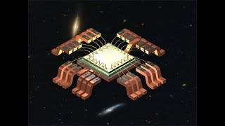
3D IC packaging refers to a technique where multiple integrated circuits (ICs) are stacked vertically to optimize space and performance. Utilizing through-silicon vias (TSVs) or microbumps for electrical connections between the layers, this technology allows for a highly compact configuration that can host numerous components within a minimal footprint. Key applications of 3D IC packaging include high-performance computing platforms, memory devices, and networking equipment.
Benefits
3D ICs offer significant advantages, including:
- Higher Performance: They minimize the distance that signals must travel, enhancing speed and efficiency.
- Lower Latency: The vertical arrangement significantly reduces the delay in signal transmission between layers.
- Reduced Interconnect Lengths: Shorter interconnects lead to lower power consumption and better signal integrity, which is crucial for applications such as artificial intelligence (AI) and machine learning.
Overall, 3D IC packaging represents a significant advancement in semiconductor technology, facilitating the development of more powerful and energy-efficient electronic devices.
Youtube Videos
Audio Book
Dive deep into the subject with an immersive audiobook experience.
Overview of 3D IC Packaging
Chapter 1 of 3
🔒 Unlock Audio Chapter
Sign up and enroll to access the full audio experience
Chapter Content
3D IC packaging involves stacking multiple ICs vertically and connecting them through through-silicon vias (TSVs) or microbumps. This allows for more components to be integrated in a smaller footprint, significantly improving performance and reducing power consumption.
Detailed Explanation
3D IC packaging is a technique where multiple integrated circuits (ICs) are layered on top of each other, rather than arranged side by side. This vertical stacking is made possible by connecting the ICs with tiny conductive pathways called through-silicon vias (TSVs) or microbumps. This method allows for a compact design, maximizing the use of space and enabling a more efficient performance. Additionally, having closer connections between chips can lead to better electrical performance and reduced energy usage, which is crucial for modern electronics.
Examples & Analogies
Think of 3D IC packaging like a multi-layered cake. Instead of spreading your favorite ingredients on a flat plate (the traditional way), you stack them in layers. Each layer adds flavor and efficiency to the cake while occupying less horizontal space. Just as it’s easier to carry a stacked cake than multiple plates of ingredients, 3D ICs offer a more efficient solution for modern electronics.
Applications of 3D IC Packaging
Chapter 2 of 3
🔒 Unlock Audio Chapter
Sign up and enroll to access the full audio experience
Chapter Content
3D ICs are used in applications such as high-performance computing, memory devices, and networking equipment.
Detailed Explanation
3D IC packaging is highly valuable in areas requiring advanced computing capabilities, such as high-performance computing systems (like supercomputers) and memory devices (such as RAM in computers). The ability to stack multiple chips in a single package facilitates faster data transfer and overall enhanced performance. Additionally, networking equipment that needs to send and receive data quickly and efficiently also benefits from this technology.
Examples & Analogies
Imagine a busy highway with many cars trying to pass through a single toll booth. If there are only one or two lanes, traffic will get backed up. However, if you have multiple levels or decks of toll booths (like a stacked toll plaza), cars can pass through simultaneously, promoting faster movement. Similarly, 3D IC packaging allows multiple data paths to operate simultaneously, speeding up processes in computing systems.
Benefits of 3D IC Packaging
Chapter 3 of 3
🔒 Unlock Audio Chapter
Sign up and enroll to access the full audio experience
Chapter Content
3D ICs offer higher performance, lower latency, and reduced interconnect lengths, making them ideal for applications in artificial intelligence (AI) and machine learning.
Detailed Explanation
One of the major benefits of 3D IC packaging is its ability to enhance performance. By reducing the distance that signals need to travel between the stacked ICs, latency—the time it takes for data to move from one point to another—is lowered. This is especially important in fields like artificial intelligence (AI) and machine learning, where quick processing of vast amounts of data is crucial for effective learning and decision-making. In addition, the overall efficiency improves, leading to better power management, which is important for battery-operated devices.
Examples & Analogies
Think of low latency like the speed of communication between two friends texting each other. If they are sitting next to each other, their messages arrive almost instantly. However, if they are far apart, it takes longer for messages to travel between them. Similarly, 3D ICs reduce the physical distance between components, allowing faster communication, which is vital in high-speed calculations needed for AI and machine learning tasks.
Key Concepts
-
3D IC Packaging: Technique for stacking ICs to optimize performance and space.
-
Through-Silicon Vias (TSVs): Vertical contacts that connect stacked ICs.
-
Lower Latency: Benefit of reducing signal travel time.
-
Microbumps: Connections used to facilitate IC stacking.
-
Interconnect Length: The distance signals travel between connections in an IC.
Examples & Applications
AI computing systems using 3D IC packaging to allow rapid data processing.
Networking equipment that benefits from reduced latency and power consumption through 3D IC architectures.
Memory Aids
Interactive tools to help you remember key concepts
Rhymes
In layers we stack, for speed that won’t lack; 3D ICs are the future, that’s a fact!
Stories
Imagine a city where everyone lives in tall skyscrapers instead of spread out on land. In that city, people travel faster because everything is close and interconnected. That’s just like 3D IC packaging!
Memory Tools
For 3D IC packaging, remember 'SHARP': Stacked, High-performance, Applications, Reduced lengths, Power efficient.
Acronyms
To remember the key benefits - 'HPLR' for Higher Performance, Lower Latency, Reduced interconnects.
Flash Cards
Glossary
- 3D IC Packaging
A method of stacking integrated circuits vertically to optimize space and electrical connections.
- ThroughSilicon Vias (TSVs)
Vertical electrical connections that pass through silicon wafers to facilitate communication between stacked ICs.
- Microbumps
Tiny solder connections used to bridge stacked ICs in a 3D packaging arrangement.
- Performance
The effectiveness and speed at which an IC function according to design specifications.
- Latency
The delay before a transfer of data begins following an instruction for its transfer.
- Interconnect Length
The physical distance between electrical connections in a circuit.
- HighPerformance Computing
Powerful computing systems designed to process large amounts of data rapidly and efficiently.
Reference links
Supplementary resources to enhance your learning experience.