
Historical Context of IC Packaging
Interactive Audio Lesson
Listen to a student-teacher conversation explaining the topic in a relatable way.
Overview of Early IC Packaging
🔒 Unlock Audio Lesson
Sign up and enroll to listen to this audio lesson

Let's start with the history of IC packaging. It all began in the 1950s when the first integrated circuits were created, primarily packaging simple germanium transistors. Who can tell me what the early packaging materials were?

They were mostly made of ceramic materials, right?
Correct! Ceramics offered durability and thermal stability. Early packages used through-hole technology, which had leads that passed through the entire package to connect to external circuits.

What about those Dual in-line Packages (DIPs)? Were they common back then?
Excellent point! DIPs became very popular as they allowed installation directly into PCBs. Remember 'DIP' as a simple method for a straight-forward chip connection!

Did military applications use different packaging?
Yes! High-reliability applications often used ceramic packages due to their robustness. Let's summarize that early IC packaging was about durability and connection efficiency.
Transition to Surface-Mount Technology
🔒 Unlock Audio Lesson
Sign up and enroll to listen to this audio lesson

Moving into the 1980s, the industry shifted toward Surface Mount Technology, or SMT. Can anyone explain what SMT allows?

It lets components be attached directly on the surface of the PCB instead of through holes!
Exactly! This greatly reduced device size and improved design flexibility. What new components resulted from this shift?
Small-outline integrated circuits like SOICs became common.
Right again! The concept of 'smaller is better' became prominent in packaging. Can anyone suggest how automation played a role?
It made the assembly process faster and more accurate.
Perfect! So, we concluded that SMT not only enhanced compactness in design but also improved manufacturing processes.
Emergence of Advanced Packaging Techniques
🔒 Unlock Audio Lesson
Sign up and enroll to listen to this audio lesson
Now, let's touch on the innovations in the 1990s, particularly BGA and flip-chip technology. Who knows what BGA stands for?
It's Ball Grid Array, right?
Correct! BGAs use solder balls for connections, enabling higher density in a smaller footprint. What advantages do you think this brings?
Better thermal performance and more pins.
Exactly! Now, can someone explain flip-chip packaging?
In flip-chip, the IC is flipped upside down for connections, allowing higher speeds.
Great! Quick recap: BGA focuses on density and thermal efficiency, while flip-chip emphasizes speed. Both revolutionized high-performance component interconnections.
Integration with SiP and SoC Technologies
🔒 Unlock Audio Lesson
Sign up and enroll to listen to this audio lesson
Finally, let's discuss SiP and SoC from the late 90s and beyond. What does SiP stand for?
System in Package!
Correct! SiP integrates multiple components into a single package. What about SoC?
That's System on Chip, integrating the entire system into one chip!
Exactly right! Mobile devices and IoT benefited greatly from these technologies. Why do you think this vertical integration is so important?
It saves space and improves efficiency.
You nailed it! So, we see how packaging evolution leads to ever more efficient and compact electronic devices.
Introduction & Overview
Read summaries of the section's main ideas at different levels of detail.
Quick Overview
Standard
The historical context of IC packaging presents an evolution from early through-hole packages in the 1950s to sophisticated methods such as System in Package (SiP) in the 2000s, reflecting advances in semiconductor technology and the demand for efficient electronic devices.
Detailed
Historical Context of IC Packaging
The history of integrated circuit (IC) packaging began in the 1950s, coinciding with the development of early integrated circuits that utilized germanium transistors. Initially, these ICs were enclosed in simple metal or ceramic packages, enhancing their durability and allowing for necessary electrical connections.
Early IC Packaging
In the early stages of semiconductor technology, through-hole packages were the norm. Made from ceramic materials, packages with leads that passed through were crucial for connecting early computers and communication devices, despite their large size.
- Dual in-line Package (DIP) became prominent for various components, offering simple integration with printed circuit boards (PCBs).
- Ceramic Packages provided exceptional reliability for industries that demanded high performance, such as military and aerospace applications.
Development of Surface Mount Technology (SMT)
In the 1980s, the advent of Surface Mount Technology (SMT) revolutionized IC packaging. This technique mounted components atop PCBs, contrasting with the older through-hole method and allowing for more compact device designs. SMT components like Small-Outline Integrated Circuits (SOICs) emerged, increasing the spacing efficiency of components. Additionally, automation in assembly was a notable advancement accompanying SMT, increasing both speed and accuracy.
BGA and Flip-Chip Packaging
The 1990s saw the introduction of more advanced packaging methods like Ball Grid Array (BGA) and Flip-Chip packaging.
- BGA provided a higher pin count, ensuring better thermal performance, ideal for high-density applications.
- Flip-Chip Packaging enhanced connectivity through the IC's surface, ideal for applications requiring significant speed.
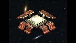
System in Package (SiP) and System on Chip (SoC)
By the end of the 1990s and into the 2000s, innovations converged on System in Package (SiP) and System on Chip (SoC) technologies, optimizing integration and miniaturization. SiP integrates various components into a single package suited for mobile devices and IoT applications. SoC technology further compresses an entire system's functionality into one chip, greatly advancing efficiency in smartphones and tablets.
This historical journey showcases the relentless pursuit of miniaturization, efficiency, and performance enhancement in IC packaging, aligning with the advancing landscape of electronic devices.
Youtube Videos
Audio Book
Dive deep into the subject with an immersive audiobook experience.
Introduction to the History of IC Packaging
Chapter 1 of 6
🔒 Unlock Audio Chapter
Sign up and enroll to access the full audio experience
Chapter Content
The history of IC packaging dates back to the 1950s when the first integrated circuits were developed. Early ICs were made using germanium transistors and were packaged in relatively simple metal or ceramic enclosures to protect and connect the chips. Over time, as silicon and miniaturization took over, packaging technologies had to evolve to meet the needs of increasingly complex and smaller devices.
Detailed Explanation
The development of integrated circuits (ICs) started in the 1950s. During this time, the first ICs were crafted using materials like germanium. These early ICs were wrapped in basic metal or ceramic cases that offered protection and connectivity. As IC technology progressed and smaller components were desired, packaging had to innovate to keep pace with these changes.
Examples & Analogies
Think of it as a phone moving from a bulky box to a slim, stylish case. In the early days, ICs needed strong but rudimentary protection—much like a thick, protective case for a new smartphone. As technology advanced, the need for sleek and compact packaging grew.
Early IC Packaging Techniques
Chapter 2 of 6
🔒 Unlock Audio Chapter
Sign up and enroll to access the full audio experience
Chapter Content
In the early days of semiconductor technology, through-hole packages were the primary method for packaging ICs. These packages were often made from ceramic materials, with leads passing through the package to make electrical connections with external circuits. These early packaging methods were large and relatively inefficient, but they were essential for the development of early computers and communication devices.
Detailed Explanation
Initially, ICs were packaged using through-hole technology, a method where components are physically placed through holes in a printed circuit board. This basic ceramic packaging had leads that connected directly to the board. Although the design was somewhat cumbersome and wide, it was crucial for the early stages of computer and communication tech development.
Examples & Analogies
Consider how older phones had large, heavy batteries that lasted long but made the phones bulky. Similarly, through-hole packaging was not sleeker or more efficient but essential for the initial steps in our technology journey.
Introduction of Dual in-line Package (DIP) and Ceramic Packages
Chapter 3 of 6
🔒 Unlock Audio Chapter
Sign up and enroll to access the full audio experience
Chapter Content
Dual in-line Package (DIP): One of the most common early IC packages, the DIP had two rows of pins that could be inserted into a printed circuit board (PCB). This was widely used for logic chips and other early components. Ceramic Packages: Many of the first ICs were packaged in ceramic enclosures due to the material’s durability and ability to withstand high temperatures. These packages were often used for high-reliability applications such as military and aerospace systems.
Detailed Explanation
The Dual In-line Package (DIP) was a popular type of packaging for early ICs, enabling easy installation on circuit boards with its two rows of pins. Similarly, robust ceramic packages were appreciated for their resistance to heat and environmental factors, making them suitable for critical functions in military and aerospace applications.
Examples & Analogies
Imagine a sturdy, waterproof bag that protects important documents. Just like this bag keeps the documents safe, ceramic packages ensured that sensitive chips remained intact in challenging environments.
Transition to Surface Mount Technology (SMT)
Chapter 4 of 6
🔒 Unlock Audio Chapter
Sign up and enroll to access the full audio experience
Chapter Content
In the 1980s, the industry began to shift toward surface-mount technology (SMT), which allowed components to be directly mounted onto the surface of the PCB rather than inserted through holes. This innovation significantly reduced the size of devices and allowed for more compact and efficient designs.
Detailed Explanation
The 1980s marked a pivotal change with the introduction of Surface Mount Technology (SMT), which changed how components were attached to circuit boards. Instead of inserting through holes, components could now be affixed directly onto the surface. This shift not only minimized the size of devices but optimized their design, enabling the creation of more compact electronics.
Examples & Analogies
Think of it like moving from a heavy, bulky computer to a lightweight laptop. Just as the laptop is easier to carry and use in different places, SMT allowed for smaller and more portable electronic devices.
Advancements with BGA and Flip-Chip Packaging
Chapter 5 of 6
🔒 Unlock Audio Chapter
Sign up and enroll to access the full audio experience
Chapter Content
In the 1990s, Ball Grid Array (BGA) and flip-chip packaging emerged as advanced packaging methods for high-performance and high-pin-count devices. Ball Grid Array (BGA): BGAs use an array of small solder balls for electrical connections between the IC and the PCB. BGAs are preferred for high-density applications because they provide a higher pin count in a smaller area and have better thermal performance compared to traditional pin-based packages. Flip-Chip Packaging: In flip-chip packaging, the IC is flipped upside down, and the electrical connections are made through bumps of solder on the chip. This allows for high-speed connections and is particularly useful in high-performance applications such as processors and graphic cards.
Detailed Explanation
The 1990s saw the rise of two advanced packaging techniques: Ball Grid Array (BGA) and flip-chip packaging. BGAs maximize surface area for connections, utilizing solder balls for dense layouts which enhance thermal efficiency and connection points. On the other hand, flip-chip processes involve flipping the IC so that the connections are made on the underside, which notably improves the speed of data transfer and is vital for high-performance electronics like CPUs and GPUs.
Examples & Analogies
Imagine a soccer team where all players huddle closely together for a free kick. Just as this gathering allows for more strategic play, BGA enables denser electronic layouts for better efficiency. Flip-chip is like a quarterback throwing the ball directly from behind the line of scrimmage—faster and more direct!
Introduction of System in Package (SiP) and System on Chip (SoC)
Chapter 6 of 6
🔒 Unlock Audio Chapter
Sign up and enroll to access the full audio experience
Chapter Content
By the late 1990s and early 2000s, the trend shifted toward System in Package (SiP) and System on Chip (SoC) technologies. These packaging technologies integrate multiple ICs and other components into a single package, providing a compact solution for complex systems. System in Package (SiP): SiP involves the integration of different chips, such as processors, memory, and sensors, into a single package, enabling high levels of integration for mobile devices, wearables, and IoT (Internet of Things) devices. System on Chip (SoC): SoC integrates the entire system, including the processor, memory, and peripherals, into a single chip. SoC technology is commonly used in smartphones, tablets, and embedded systems.
Detailed Explanation
Toward the end of the 1990s and into the 2000s, the focus of packaging shifted dramatically with System in Package (SiP) and System on Chip (SoC) technologies. SiP combines several different chips into one compact package useful for modern mobile and IoT devices. In contrast, SoC takes this a step further by embedding the entire system—including processing and memory—onto a single chip structure, which is prevalent in all of today's smartphones and tablets.
Examples & Analogies
Think of a Swiss Army knife, which integrates various tools into one compact item. Similarly, SiP and SoC bring together many electronic functions into one small package, making devices more versatile and space-saving.
Key Concepts
-
Historical Development: Explains the timeline of IC packaging from the 1950s to the 2000s.
-
Through-Hole Packaging: The early method where components were inserted through the PCB and connected.
-
Surface Mount Technology (SMT): A modern approach that allows the mounting of components on the surface of the PCB.
-
Ball Grid Array (BGA): An advanced packaging technique that enhances connection density through the use of solder balls.
-
System in Package (SiP) and System on Chip (SoC): Modern integration techniques that improve compactness and efficiency.
Examples & Applications
A Dual In-Line Package (DIP) allows easy insertion into a PCB through its rows of pins.
Using BGA packaging, a smartphone can maintain high performance while being compact in size.
Memory Aids
Interactive tools to help you remember key concepts
Rhymes
In the 1950s, chips were crude, protected in ceramics, they were good. With every leap, they found a way, to package them better, and save the day.
Stories
Imagine a small robot chip that could only work inside a cardboard box. One day it found a strong ceramic shell that not only protected it but also helped it connect to other robot friends. As robots became smarter, they started living in BGA houses that provided more room for friends, making them super close!
Memory Tools
When recalling types of packaging: Think 'DBFS' - Dual in-line, BGA, Flip-chip, SMT (the progression in packaging).
Acronyms
Remember 'SiP' as 'System in Package' - it's the key for integration in modern devices!
Flash Cards
Glossary
- IC Packaging
The process of enclosing an integrated circuit chip within a protective housing.
- DIP
Dual In-line Package, a common type of package for ICs with pins on either side.
- SMT
Surface Mount Technology, a method of mounting electronic components directly onto the surface of a PCB.
- BGA
Ball Grid Array, a type of package that uses an array of solder balls for connections.
- FlipChip
A packaging method where an integrated circuit is mounted upside down, with connections made through solder bumps.
- SiP
System in Package, a technology that integrates multiple components into a single package.
- SoC
System on Chip, a method of integrating a complete system onto a single chip.
Reference links
Supplementary resources to enhance your learning experience.