
Evolution of IC Packaging Technologies
Interactive Audio Lesson
Listen to a student-teacher conversation explaining the topic in a relatable way.
Introduction to IC Packaging Evolution
🔒 Unlock Audio Lesson
Sign up and enroll to listen to this audio lesson

Today, we will explore the evolution of IC packaging technologies. Can anyone tell me why IC packaging is critical?

It protects the IC, right? And helps connect it to other parts.
Exactly, Student_1! IC packaging provides crucial protection and electrical interfacing. As devices get smaller and more powerful, we need advanced packaging methods. What might some of these new methods be?

Maybe 3D IC packaging?
Great mention, Student_2! 3D IC packaging allows us to stack chips vertically which minimizes space. Can anyone recall the benefits of this method?

It can improve performance and reduce power use.
That's right! Summarizing this, 3D IC packaging enhances performance and facilitates miniaturization, critical for modern applications.
Exploring Fan-Out Wafer-Level Packaging
🔒 Unlock Audio Lesson
Sign up and enroll to listen to this audio lesson

Now, let’s discuss Fan-Out Wafer-Level Packaging or FOWLP. Someone tell me how this technology works!

Is it where they put chips into a wafer and spread them out?
Exactly, Student_4! By embedding chips in a reconstituted wafer, FOWLP can fan out connections. What advantages do you think this brings?
It probably allows for better cooling and lower costs?
Correct! FOWLP offers improved thermal performance and cost efficiencies, especially useful in mobile and IoT devices. Let’s summarize: FOWLP is innovative for its high density and thermal capabilities!
Introduction & Overview
Read summaries of the section's main ideas at different levels of detail.
Quick Overview
Standard
The evolution of IC packaging technologies is driven by the need for more powerful and energy-efficient devices. Key innovations include 3D IC packaging and Fan-Out Wafer-Level Packaging, which provide increased performance and integration for high-demand applications across various industries.
Detailed
Evolution of IC Packaging Technologies
As the demand for smaller, powerful, and energy-efficient devices increases, IC packaging technologies have evolved significantly. This section highlights the development of several advanced packaging methods central to modern electronics:
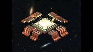
1. 3D IC Packaging
3D IC packaging stacks multiple integrated circuits (ICs) vertically and connects them through innovative techniques like through-silicon vias (TSVs) or microbumps. This arrangement allows for more components to fit in a smaller footprint, improving performance and reducing power consumption.
Applications:
3D ICs are predominantly used in high-performance computing, memory devices, and networking equipment.
Benefits:
They offer higher performance, lower latency, and shorter interconnect lengths, making them ideal for AI and machine learning applications.
2. Fan-Out Wafer-Level Packaging (FOWLP)
FOWLP is an advanced technique where integrated circuits are embedded in a reconstituted wafer, fanning out connections from the chip to a larger package.
Applications:
This method is widely applied in mobile devices, IoT devices, and wearables.
Benefits:
It enables higher density packaging with enhanced thermal performance and cost efficiencies compared to traditional packaging methods.
In summary, continued advancements in IC packaging are crucial as they cater to evolving technological demands, leading to more compact and efficient electronic solutions.
Youtube Videos
Audio Book
Dive deep into the subject with an immersive audiobook experience.
Introduction to Evolution
Chapter 1 of 3
🔒 Unlock Audio Chapter
Sign up and enroll to access the full audio experience
Chapter Content
As the demand for smaller, more powerful, and energy-efficient devices has increased, IC packaging technologies have had to evolve. Today, the packaging industry is exploring several advanced packaging methods to meet the growing needs of high-performance computing, telecommunications, and consumer electronics.
Detailed Explanation
This chunk introduces the key theme of the evolution of IC packaging technologies. It explains that the increasing demand for smaller and more efficient devices has prompted significant changes in how integrated circuits (ICs) are packaged. As technology advances, especially in fields like computing and telecommunications, packaging methods must adapt to support these changes.
Examples & Analogies
Think of packaging in the technology industry like the evolution of food packaging. Just as food products have shifted from bulky plastic containers to sleek, eco-friendly designs that reflect consumer demand for convenience and sustainability, IC packaging has similarly become more sophisticated to meet the demands of modern electronics.
3D IC Packaging
Chapter 2 of 3
🔒 Unlock Audio Chapter
Sign up and enroll to access the full audio experience
Chapter Content
3D IC packaging involves stacking multiple ICs vertically and connecting them through through-silicon vias (TSVs) or microbumps. This allows for more components to be integrated in a smaller footprint, significantly improving performance and reducing power consumption.
Detailed Explanation
3D IC packaging is a technique where multiple integrated circuits are stacked on top of each other rather than arranged side by side. Through-silicon vias (TSVs) or microbumps are used to connect these stacked ICs, which allows for a much denser configuration. This method leads to improved performance because the connections between the chips are shorter, resulting in reduced power consumption and greater efficiency, particularly in applications like artificial intelligence and high-performance computing.
Examples & Analogies
Imagine a three-story apartment building where each floor houses different functions yet are all interconnected. If a person on the first floor wants to communicate with someone upstairs, they have a shorter distance to travel via a staircase compared to if they had to run down and outside to connect with someone in a different building. Similarly, 3D IC packaging shortens the distance between ICs, enhancing speed and efficiency.
Fan-Out Wafer-Level Packaging (FOWLP)
Chapter 3 of 3
🔒 Unlock Audio Chapter
Sign up and enroll to access the full audio experience
Chapter Content
Fan-Out Wafer-Level Packaging (FOWLP) is an advanced packaging technique that involves embedding ICs in a reconstituted wafer and fanning out the connections from the chip to a larger package. This technology allows for higher density, better thermal performance, and lower costs compared to traditional packaging methods.
Detailed Explanation
FOWLP is a modern approach to packaging integrated circuits that allows for more compact designs. In this method, ICs are embedded within a specially designed wafer. The connections are then distributed or ‘fanned out’ from the chip to a larger package. This not only increases the density of components but also improves thermal performance—meaning the chips can operate more efficiently and with less heat generation. Moreover, it tends to be more cost-effective than older packaging methods due to material efficiency and manufacturing processes.
Examples & Analogies
Think of FOWLP like a family tree where each branch leads to a different family member. Instead of everyone living separately in their own houses (like traditional packaging), they’re all connected on a big tree that allows for fast and efficient communication among family members. This compact connection reduces the space taken up and improves family gatherings — just as FOWLP reduces space and enhances performance in electronic devices.
Key Concepts
-
IC Packaging: The process of enclosing an IC chip in a protective housing to facilitate connections.
-
3D IC Packaging: A method that allows stacking ICs vertically for enhanced performance and efficiency in device design.
-
Fan-Out Wafer-Level Packaging: A technique that embeds ICs in a larger package through reconstituted wafers, maximizing density and minimizing costs.
Examples & Applications
3D IC packaging is used in high-performance computing systems to reduce latency and enhance speed.
FOWLP is commonly found in IoT devices due to its compact form and thermal efficiency.
Memory Aids
Interactive tools to help you remember key concepts
Rhymes
3D stacks up high, saves space as time flies, with chips stacked so neat, performance can't be beat!
Stories
Imagine a city building taller upwards rather than wider; just like this, 3D ICs enable devices to be more powerful without needing more land!
Memory Tools
Remember 'FOWLP': Flexible in design, Optimal for performance, Weight-saving, Lingo of connectivity, Power-friendly.
Acronyms
Use '3D' for 'Densely Designed Devices' to remember the impact of 3D IC packaging.
Flash Cards
Glossary
- 3D IC Packaging
A packaging method that stacks multiple integrated circuits vertically to connect them more efficiently.
- FanOut WaferLevel Packaging (FOWLP)
An advanced packaging technique where ICs are embedded in a reconstituted wafer and connections are fanned out.
- ThroughSilicon Vias (TSVs)
Vertical connections passing through silicon wafers to enable vertical stacking of ICs.
Reference links
Supplementary resources to enhance your learning experience.