
Low Power Design Strategies and Techniques in Advanced Technologies
Enroll to start learning
You’ve not yet enrolled in this course. Please enroll for free to listen to audio lessons, classroom podcasts and take practice test.
Interactive Audio Lesson
Listen to a student-teacher conversation explaining the topic in a relatable way.
Core Principles of Low Power Design
🔒 Unlock Audio Lesson
Sign up and enroll to listen to this audio lesson

Let's begin by discussing the core principles of low power design. The first principle is to minimize the supply voltage, known as Vdd. Why do you think lowering the Vdd is important?

I think it helps reduce power because dynamic power is proportional to Vdd squared.
Correct! However, we must balance it out because lowering Vdd can affect performance and noise margins. What do you understand about switching activity, α?

Switching activity refers to how often the logic states change, right? Lowering that will also save power.
Exactly! We can achieve this by utilizing encoding schemes or gating signals. Remember: less switching means less dynamic power. Let’s move on to managing capacitance; how can a lower capacitance help?

If we lower capacitance, we can reduce the total power consumption in the circuit.
Great! Optimizing layout is key here. Lastly, reducing frequency can be effective, too. Who can tell me how clock gating fits into this?

Clock gating disables the clock to parts of the circuit that aren't in use, which saves power!
Exactly right! Remember these principles, as they are essential for effective low power design.
Techniques in CMOS-Based Digital Circuits
🔒 Unlock Audio Lesson
Sign up and enroll to listen to this audio lesson

Now, let’s focus on techniques specifically for CMOS-based digital circuits. Who can explain what DVFS stands for?
DVFS stands for Dynamic Voltage and Frequency Scaling, which adjusts voltage and frequency based on workload.
Well done! It’s widely used in processors and SoCs. What about clock gating? How does that contribute to power savings?
It stops the clock to sections of the circuit that aren’t active, so it cuts out unnecessary power use.
Exactly! Can anyone explain how Multi-Vt designs work?
They mix high-Vt and low-Vt transistors to balance between leakage and performance.
Good point! Multi-Vt designs help optimize power efficiency. Finally, what do we mean by power gating?
Power gating disconnects portions of the circuit using sleep transistors when they're not in use.
Exactly! Anyone here want to jump in and explain subthreshold logic?
It allows operation in the subthreshold region for ultra-low power applications, like IoT devices.
Excellent summary! Understanding these concepts enables better low power design in advanced technologies.
Low Power Techniques in Analog Circuits
🔒 Unlock Audio Lesson
Sign up and enroll to listen to this audio lesson
Now we will discuss low power techniques in analog circuits. Why do you think Vdd can't be scaled down as aggressively in analog circuits?
Because signal integrity suffers, making it harder to maintain the correct output signals.
True! Let’s talk about current reuse. How does that help save power?
By reusing the current from one bloc instead of generating it again, power consumption can be lowered.
Correct! And what about bias optimization? What do you think that entails?
Using adaptive biasing based on the signal level to minimize power as needed?
Exactly right! Now, could someone elaborate on switched capacitor techniques?
They replace resistors with capacitors for filtering, which saves a lot of power.
Spot on! Finally, what should we know about low-voltage amplifier architectures?
They require specific designs like folded cascode or telescopic to work effectively at low voltages.
Great insights! These strategies are essential for developing efficient low-power analog circuits.
Combined Strategies for SoC-Level Power Management
🔒 Unlock Audio Lesson
Sign up and enroll to listen to this audio lesson
To wrap up, let’s discuss combined strategies for power management at the SoC level. Why is this integration necessary?
It ensures a holistic approach to manage power more effectively across all components.
Exactly! What are some strategies here for digital circuits?
For digital circuits, we can use DVFS, clock gating, and multi-Vt cell designs.
Awesome! And what about memory techniques?
We could employ bitline segmentation and shutdowns for sense amplifiers to lower power use.
Great examples! Let’s not forget about analog strategies. Anyone know what they might include?
Current reuse and dynamic biasing would be essential for the analog sections.
Yes! Finally, how could system-level techniques apply here?
Techniques like adaptive voltage scaling can help us manage power based on workload.
Great wrap-up! Each of these strategies contributes to efficient power management in modern SoCs.
Introduction & Overview
Read summaries of the section's main ideas at different levels of detail.
Quick Overview
Standard
As device scaling approaches atomic limits, this chapter explores advanced methods for reducing dynamic and static power consumption in integrated circuits while maintaining performance and reliability. Techniques cover various levels of design, including device, circuit, architecture, and system level.
Detailed
Low Power Design Strategies and Techniques in Advanced Technologies
Introduction
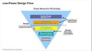
This chapter delves into advanced strategies and techniques aimed at minimizing power consumption in modern CMOS and FinFET-based integrated circuits. With device scaling reaching atomic limits, power constraints are crucial in design decisions, compelling engineers to integrate sophisticated methods across various levels including device, circuit, architecture, and system levels. A tailored approach is essential for both digital and analog circuits to achieve low power while fulfilling performance, area, and reliability requirements.
Problem Statement
One of the primary challenges is to effectively reduce both dynamic and static power consumption across varied operating conditions without compromising performance or significantly increasing cost and area. Key issues in deeply scaled technologies include the exponential growth of leakage currents, conflicts between dynamic power reduction and speed, and analog circuits’ susceptibility to reduced voltage headroom and poor linearity, necessitating multi-domain techniques.
Core Principles of Low Power Design
- Minimize Supply Voltage (Vdd): Dynamic power and leakage are affected exponentially by supply voltage, but lowering Vdd may sacrifice performance and noise margins.
- Reduce Switching Activity (α): Implementing encoding schemes and signal gating can decrease unnecessary transitions.
- Lower Capacitance (C): Optimizing layout, interconnects, and minimizing gate sizes or using fewer buffers can effectively manage capacitance.
- Reduce Frequency (f): Techniques like clock gating and dynamic frequency scaling help manage power efficiently.
- Leakage Management: This includes methods like power gating and multi-Vt cells to control leakage effects.
Techniques in CMOS-Based Digital Circuits
Noteworthy techniques include Dynamic Voltage and Frequency Scaling (DVFS) for runtime adjustments, clock gating to disable idle blocks, Multi-Vt designs for mixed transistor types, and power gating for subsystem management. Operand isolation and subthreshold logic are also key for managing power consumption effectively.
FinFET-Specific Power Strategies
FinFETs enhance power efficiency but require specialized strategies such as Near-Threshold Computing (NTC), adjusting threshold voltages dynamically via back biasing, and employing custom cell libraries to accommodate low Vdd operations.
Low Power Techniques in Analog Circuits
Analog circuits necessitate unique strategies, including current reuse and bias optimization, as well as switched capacitor techniques and low-voltage architectures to maintain signal integrity while saving power.
Combined Strategies for SoC-Level Power Management
Integrative strategies combine techniques across digital and analog domains, memory handling, and system-level approaches to manage power consumption comprehensively.
Python Simulation
A simulation example demonstrates the power impact of DVFS on dynamic power under different voltage conditions. This emphasizes the practical applications of power-saving techniques in real-world scenarios.
Conclusion
Effective low-power design mandates a multi-faceted approach combining voltage and frequency scaling, gating techniques, and smart biasing strategies. By tailoring designs to specific applications, designers can maximize efficiency in power-critical environments.
Youtube Videos


Audio Book
Dive deep into the subject with an immersive audiobook experience.
Introduction to Low Power Design
Chapter 1 of 6
🔒 Unlock Audio Chapter
Sign up and enroll to access the full audio experience
Chapter Content
This chapter discusses advanced strategies and design techniques to minimize power consumption in modern CMOS and FinFET-based integrated circuits. As device scaling approaches atomic limits and power constraints dominate design decisions, engineers must adopt sophisticated methods at the device, circuit, architecture, and system levels. Both digital and analog circuits require customized approaches to achieve low power while maintaining performance, area, and reliability requirements.
Detailed Explanation
In this introduction, the focus is on the need for low power design in integrated circuits, particularly as technology advances. As chips become smaller and more complex, the challenge of managing power consumption increases. Engineers must implement various strategies that address this issue, ensuring that the performance of circuits is not compromised. This includes tailored approaches for both digital and analog circuits, emphasizing the importance of balancing power, performance, size, and reliability.
Examples & Analogies
Think of low power design like designing a fuel-efficient car. Just as automotive engineers must find ways to minimize fuel consumption while maximizing speed and safety, electrical engineers must reduce power usage in chips while ensuring they perform efficiently.
Problem Statement in Low Power Design
Chapter 2 of 6
🔒 Unlock Audio Chapter
Sign up and enroll to access the full audio experience
Chapter Content
The key challenge is to reduce both dynamic and static power consumption across operating conditions without compromising performance or increasing cost and area significantly. In deeply scaled technologies:
● Leakage currents grow exponentially.
● Dynamic power reduction conflicts with speed.
● Analog blocks suffer from reduced voltage headroom and poor linearity.
Hence, multi-domain techniques are necessary.
Detailed Explanation
The problem statement outlines critical challenges in managing power consumption. Dynamic power, which increases with speed, must be balanced against static power, which grows due to leakage currents. As technologies advance and components shrink, leakage becomes a larger issue. Additionally, analog components face their unique issues, providing less voltage to work with, which affects their performance. This creates a need for comprehensive solutions that consider multiple aspects of design.
Examples & Analogies
Imagine a smartphone with a battery that drains too quickly. To extend battery life, manufacturers might need to balance faster processors with better efficiency, just like engineers balancing power and performance in circuit design.
Core Principles of Low Power Design
Chapter 3 of 6
🔒 Unlock Audio Chapter
Sign up and enroll to access the full audio experience
Chapter Content
- Minimize Supply Voltage (Vdd):
- Dynamic power ∝ V2
- Leakage ∝ e−Vt/Vth
- But reducing Vdd reduces performance and noise margins.
- Reduce Switching Activity (α):
- Use encoding schemes, signal gating, and efficient logic styles.
- Lower Capacitance (C):
- Optimize layout and interconnects.
- Use smaller gates and fewer buffers.
- Reduce Frequency (f):
- Employ clock gating and dynamic frequency scaling.
- Leakage Management:
- Power gating, multi-Vt cells, body biasing.
Detailed Explanation
This section outlines the fundamental principles for achieving low power design: 1) Reducing supply voltage lowers both dynamic and leakage power but may hinder performance. 2) Managing switching activity, or how often components change states, is crucial for reducing power use. 3) Lowering capacitance in components minimizes power loss. 4) Lowering the operating frequency can help save energy through techniques like clock gating. 5) Finally, managing leakage through various strategies ensures that unnecessary power drain is minimized.
Examples & Analogies
It's like trying to reduce water usage in a shower. Lowering the water pressure can save water but could make it less effective. Similarly, reducing power voltage can save power but might affect performance.
Techniques in CMOS-Based Digital Circuits
Chapter 4 of 6
🔒 Unlock Audio Chapter
Sign up and enroll to access the full audio experience
Chapter Content
- Dynamic Voltage and Frequency Scaling (DVFS):
- Adjusts voltage and frequency at runtime based on workload.
- Used in processors, SoCs, and smartphones.
- Clock Gating:
- Disables clock to idle functional blocks to reduce dynamic power.
- Multi-Vt Design:
- Combines high-Vt (low leakage, slow) and low-Vt (fast, leaky) transistors.
- Power Gating:
- Disconnects blocks using sleep transistors when not in use.
- Saves leakage at the cost of wake-up latency.
- Operand Isolation:
- Prevents unnecessary switching in data paths.
- Subthreshold Logic:
- Operates transistors in subthreshold region for ultra-low-power (IoT). Example: ARM Cortex-M series uses DVFS + power gating + clock gating for ultra-low-power embedded processing.
Detailed Explanation
This section presents various techniques focusing on CMOS-based circuits. 1) DVFS helps manage power dynamically. 2) Clock gating saves energy by turning off sections of the circuit when not in use. 3) Multi-Vt design mixes transistors with different characteristics for optimal performance. 4) Power gating keeps circuits off when not in use, although this introduces delays when reactivating them. 5) Operand isolation limits unnecessary data processing. 6) Subthreshold logic provides extreme power savings for small devices, like IoT sensors.
Examples & Analogies
Consider a smart thermostat that adjusts its heating power based on whether people are home or not – that's DVFS in action, optimizing power usage based on current need.
Low Power Techniques in Analog Circuits
Chapter 5 of 6
🔒 Unlock Audio Chapter
Sign up and enroll to access the full audio experience
Chapter Content
Analog circuits cannot scale Vdd aggressively due to signal integrity. Power-saving methods include:
1. Current Reuse:
- Reuse current in multiple blocks (e.g., gm boosting techniques).
2. Bias Optimization:
- Use low-current biasing, adaptive biasing based on signal level.
3. Switched Capacitor Techniques:
- Eliminate power-hungry resistors using capacitive filtering.
4. Low-Voltage Amplifier Architectures:
- Folded cascode, telescopic op-amps, inverter-based op-amps.
5. Programmable Gain Blocks (PGAs):
- Use digital control to reduce gain stages when not required.
Example: Low-power biomedical devices use subthreshold biasing in analog front ends to extend battery life.
Detailed Explanation
In analog circuits, maintaining signal quality while also cutting down power usage is challenging. This section outlines strategies to minimize power consumption without compromising the signal's integrity. Techniques like current reuse enhance efficiency by reducing redundant current use across components. Bias optimization and switched capacitor techniques improve efficiency by minimizing energy use during signal processing. Low-voltage amplifier designs enable analog components to operate at lower power levels, while PGAs adapt dynamically to reduce unnecessary amplification.
Examples & Analogies
Imagine a water filtration system that can share its water flow for multiple purposes instead of using separate taps for each. Current reuse works similarly, maximizing energy efficiency.
FinFET-Specific Power Strategies
Chapter 6 of 6
🔒 Unlock Audio Chapter
Sign up and enroll to access the full audio experience
Chapter Content
FinFETs inherently improve efficiency due to better gate control, but they still require design techniques:
1. Near-Threshold Computing (NTC):
- Operates at voltages close to threshold (~0.3–0.5V).
- Achieves massive power savings at the cost of speed.
2. Back Biasing (Dynamic Body Biasing):
- Adjusts threshold voltage dynamically to manage performance/leakage trade-offs.
3. Fine-Grain Power Domains:
- Divides SoC into small blocks with independent power rails.
- Reduces leakage and enables aggressive DVFS.
4. Custom Cell Libraries:
- FinFET standard cells designed for ultra-low Vdd operation.
- Trade-off between drive strength and leakage.
Detailed Explanation
This section focuses on strategies tailored for FinFET technology, which offers improved efficiency. 1) Near-Threshold Computing allows operations at very low voltages, providing power savings. However, this comes at the cost of speed. 2) Dynamic body biasing helps manage trade-offs between power leakage and performance. 3) Fine-grain power domains enhance energy efficiency by enabling different chip areas to operate independently in terms of power. 4) Custom cell libraries are designed specifically for low voltage operation.
Examples & Analogies
Think of turning down the brightness of a smartphone screen to save battery while still being able to use the device efficiently. Near-Threshold Computing is similar, reducing power consumption while sacrificing some performance.
Key Concepts
-
Dynamic Power: Power consumed during switching states.
-
Static Power: Power consumed when idle due to leakage.
-
DVFS: An energy-efficient method for voltage and frequency adjustment.
-
Power Gating: A technique to reduce leakage by turning off unused blocks.
-
Subthreshold Logic: Low-power logic operation below the transistor threshold voltage.
Examples & Applications
The ARM Cortex-M series uses DVFS in conjunction with power gating and clock gating to achieve ultra-low power in embedded systems.
Biomedical devices often utilize subthreshold biasing techniques in analog front ends, extending battery life.
Memory Aids
Interactive tools to help you remember key concepts
Rhymes
In low power’s quest, we must invest, minimize Vdd, and switch less, for power is best!
Stories
Imagine you’re an engineer building a tiny city. Every time a street lamp (a circuit) is on, it consumes power. If you turn off lamps not in use (clock gating) and choose energy-efficient ones (multi-Vt), your city thrives with less energy waste, just like circuits.
Memory Tools
Remember PEACE: Performance, Efficiency, Area, Cost, and Energy to balance in low-power design.
Acronyms
C2S3F
Capacitance
Clock gating
Subthreshold
Supply voltage
Frequency adjustments – key strategies for low power.
Flash Cards
Glossary
- Dynamic Power
Power consumed when a circuit is active and switching states.
- Static Power
Power consumed by a circuit when not switching states, primarily due to leakage currents.
- DVFS
Dynamic Voltage and Frequency Scaling, a technique to adjust voltage and frequency based on the workload.
- Leakage Currents
Unwanted currents that flow through a device when it is off or idle, leading to static power consumption.
- FinFET
A type of transistor that offers better control of the channel, allowing for lower power consumption in advanced technologies.
Reference links
Supplementary resources to enhance your learning experience.