
Key Design Considerations
Interactive Audio Lesson
Listen to a student-teacher conversation explaining the topic in a relatable way.
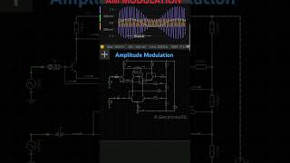
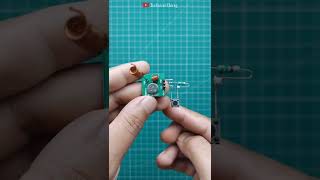
Component Selection in RF Design
🔒 Unlock Audio Lesson
Sign up and enroll to listen to this audio lesson

Today, we're focusing on the first key design consideration: component selection. Choosing components with low parasitics and high quality factors is vital for effective RF performance.

What do you mean by low parasitics, and why is it important?
Great question! Low parasitics help minimize unintended effects like noise and signal loss. Can anyone tell me an example of how parasitics can impact circuit performance?

I think parasitic capacitance can cause unwanted coupling between components!
Exactly! That's precisely why we need to be careful. Remember, 'low parasitics, high performance!'
Importance of PCB Layout
🔒 Unlock Audio Lesson
Sign up and enroll to listen to this audio lesson

Now let's discuss PCB layout. Why do you think a PCB layout is crucial for RF circuits?

Maybe because it affects interference and signal integrity?
Absolutely right! Proper PCB layout minimizes interference. Can anyone think of specific layout strategies that could be effective?

Using ground planes and controlling trace widths could help reduce noise!
Spot on! 'Ground first, noise later' is a mantra to remember when designing PCBs for RF applications.
Thermal Management in RF Circuits
🔒 Unlock Audio Lesson
Sign up and enroll to listen to this audio lesson
Finally, let's talk about thermal management. Why is managing heat important in RF circuits?
If they get too hot, components might fail or work inefficiently?
Exactly! Effective thermal management ensures components operate within safe limits. Can anyone suggest some techniques for thermal management?
Using heat sinks or thermal vias could help distribute heat!
That's right! Remember 'cool circuits create reliability.'
Introduction & Overview
Read summaries of the section's main ideas at different levels of detail.
Quick Overview
Standard
Effective RF circuit design is influenced by several key considerations, including the selection of components with low parasitics and high Q factors, careful PCB layout to minimize interference, and the implementation of thermal management strategies. These factors ensure optimal performance and reliability in high-frequency environments.
Detailed
Key Design Considerations
This section discusses essential design considerations that play a crucial role in ensuring effective RF performance. The following key aspects are covered:
Component Selection
Choosing components with low parasitics, high quality (Q) factors, and minimal loss tangents is crucial for optimal performance in RF circuits. The quality factor significantly influences the energy loss, thereby affecting overall circuit efficiency.
PCB Layout
Effective radio frequency (RF) circuit design necessitates meticulous PCB layout. This includes minimizing signal degradation, interference, and unwanted parasitic effects. Ground planes, trace width, and via placement are critical in this context.
Thermal Management
Thermal management is particularly important in high-power RF circuits, where significant heat generation is common. Techniques such as using heat sinks or thermal vias are often required to manage heat dissipation effectively. Proper thermal management helps to enhance the reliability and performance of RF systems.
Youtube Videos


Audio Book
Dive deep into the subject with an immersive audiobook experience.
Component Selection
Chapter 1 of 3
🔒 Unlock Audio Chapter
Sign up and enroll to access the full audio experience
Chapter Content
● Component Selection: Choosing components with low parasitics, high Q factors, and minimal loss tangents is crucial for effective RF performance.
Detailed Explanation
Component selection is vital in RF circuit design. Components such as resistors, capacitors, and inductors can affect the circuit's performance significantly. When selecting these components, designers look for those with low parasitics—that is, the unintended effects that can arise from their physical properties at high frequencies. A high Quality (Q) factor indicates that a component can efficiently store and release energy with minimal loss, which is particularly important in RF circuits where signal integrity is paramount. Additionally, components with minimal loss tangents mean less energy is wasted during operation, improving overall circuit performance.
Examples & Analogies
Think of component selection like choosing the right tools for a job. If you were building a treehouse, you wouldn't want to use dull saws or rusty nails. Just as sharp tools help you finish the job quickly and safely, high-quality components help RF circuits function effectively without unwanted noise or energy loss.
PCB Layout
Chapter 2 of 3
🔒 Unlock Audio Chapter
Sign up and enroll to access the full audio experience
Chapter Content
● PCB Layout: High-frequency circuits require careful PCB layout to minimize interference, signal degradation, and parasitic effects. Ground planes, trace width, and via placement are critical factors in RF PCB design.
Detailed Explanation
PCB layout is a key aspect of RF circuit design. At high frequencies, signals can be easily disrupted by interference, leading to degraded performance. To combat this, RF designers focus on creating a layout that minimizes these issues. Employing a ground plane helps to provide a stable reference for signals, reducing noise. The width of the traces (the paths on the board where current flows) also matters: wider traces can carry more current but can also introduce unwanted inductance. Additionally, the placement of vias (the holes that connect different layers of the PCB) needs to be strategic to maintain signal integrity. Every detail in the layout can drastically affect the performance of the final circuit.
Examples & Analogies
Imagine a crowded highway during rush hour. If some lanes are open and clear while others are blocked, traffic flows smoothly where the lanes are clear. Similarly, a well-designed PCB layout can ensure that signals travel without interruption, while a poor layout can cause bottlenecks that lead to interference and signal degradation.
Thermal Management
Chapter 3 of 3
🔒 Unlock Audio Chapter
Sign up and enroll to access the full audio experience
Chapter Content
● Thermal Management: High-power RF circuits may generate significant heat, so thermal management techniques, such as heat sinks or thermal vias, are often necessary.
Detailed Explanation
In RF circuits that operate at high power, managing heat is crucial because excess heat can damage components and lead to circuit failure. Thermal management involves implementing techniques to keep temperatures within safe limits. Heat sinks are often added to dissipate heat away from components, while thermal vias are used to transfer heat from one layer of the PCB to another. Proper thermal management not only helps in maintaining the functionality and longevity of the circuit but also improves overall reliability by ensuring that components operate under optimal conditions.
Examples & Analogies
Consider how your laptop manages heat. If you run a graphically intense game, it might heat up quickly. Laptops are designed with fans and heat sinks to keep the temperature down. Similarly, in RF circuits, thermal management strategies make sure components don’t overheat, enabling reliable performance even under high-demand situations.
Key Concepts
-
Component Selection: Choosing components with low parasitics and high Q factors is essential for effective RF design.
-
PCB Layout: The physical design of the PCB includes factors like ground planes and trace widths, affecting overall circuit performance.
-
Thermal Management: Proper management of thermal dissipation is critical in high-power RF circuits to maintain reliability.
Examples & Applications
Example of poor layout can lead to increased signal loss due to parasitic effects, while a well-designed PCB layout optimizes performance.
Using high-Q inductors in a filter circuit reduces energy losses, enhancing signal quality.
Memory Aids
Interactive tools to help you remember key concepts
Rhymes
Choose your parts, make them bright, low parasitics keep signals right!
Stories
Imagine an RF circuit designed poorly, with components scattered wide and free. The signals become weak and blurry, teaching us to choose wisely to ensure clarity!
Memory Tools
Remember 'CPT': Component selection, PCB layout, Thermal management for RF success.
Acronyms
To remember the key design considerations, think of 'CPTM' (Component, PCB, Thermal Management).
Flash Cards
Glossary
- Parasitics
Unwanted effects in an electronic component that can influence circuit performance, such as parasitic capacitance and inductance.
- PCB Layout
The physical arrangement of components and connections on a printed circuit board, which can significantly impact signal integrity and performance.
- Thermal Management
Techniques used to control the temperature of a circuit to ensure reliable operation, including heat sinks and thermal vias.
- Quality Factor (Q)
A measure of the energy loss in a passive component, where a higher Q represents lower loss and better performance.
Reference links
Supplementary resources to enhance your learning experience.