
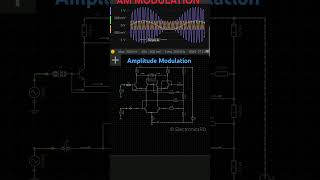
RF Circuit Design Challenges
Interactive Audio Lesson
Listen to a student-teacher conversation explaining the topic in a relatable way.
Signal Integrity
🔒 Unlock Audio Lesson
Sign up and enroll to listen to this audio lesson

Today, we're focusing on **signal integrity**. Maintaining the quality of the signal during transmission is crucial in RF designs. Who can tell me why signal integrity is so important?

I think it’s important because if the signal isn’t clear, the communication can fail.
Exactly! Noise, distortion, and reflection can degrade the signal. Remember the acronym 'NDR': Noise, Distortion, Reflection—the three main threats to signal integrity. How can we minimize these issues?

Maybe we should use shielding or filtering?
Yes, shielding and filtering are good approaches. Proper component placement and layout can also help. Let's move on to discuss component parasitics.
Component Parasitics
🔒 Unlock Audio Lesson
Sign up and enroll to listen to this audio lesson

Now, let’s talk about **component parasitics**. What do we mean by that? Who can explain?

Parasitics are the unintended effects that components have, like extra capacitance or inductance?
Exactly! Parasitic capacitance and inductance can disrupt the intended signal path. Remember, ‘More is Less’—more parasitics can lead to less performance! Can anyone give an example?

Using long leads on resistors can cause inductance!
Great example! Keeping components close together can help reduce these effects.
Power Losses
🔒 Unlock Audio Lesson
Sign up and enroll to listen to this audio lesson
Let’s discuss **power losses** next. Can anyone tell me why power loss becomes more significant at higher frequencies?
Does it have to do with resistance increasing or other inefficiencies?
Exactly. As frequency increases, the resistance can increase due to effects like the skin effect. We need efficient designs to minimize this. Why do you think this is important for RF systems?
If we lose power, it can reduce the range or performance of the device.
Spot on! This leads us to our final point—size and packaging.
Size and Packaging
🔒 Unlock Audio Lesson
Sign up and enroll to listen to this audio lesson
Finally, let’s tackle **size and packaging**. In modern applications—especially in mobile devices—why is the size so critical?
Because smaller devices are more portable and convenient!
Exactly! However, a compact design can lead to unwanted parasitics. What are some strategies we can use for effective packaging?
Routing traces carefully and using ground planes can help minimize those effects.
Great answers! Remember, managing component placement and thermal considerations will also contribute to better performance.
Introduction & Overview
Read summaries of the section's main ideas at different levels of detail.
Quick Overview
Standard
Designing RF circuits poses several challenges that are crucial to ensuring performance in high-frequency environments, such as maintaining signal integrity, addressing parasitic effects, reducing power losses, and optimizing size and packaging for practical applications.
Detailed
RF Circuit Design Challenges
Designing RF circuits involves addressing a variety of significant challenges that arise in high-frequency environments. These challenges include maintaining signal integrity to minimize noise, distortion, and reflection, which can impact the quality of the transmitted signals. Additionally, the parasitics associated with components, such as parasitic inductance, capacitance, and resistance, must be carefully considered to avoid unintended influences on signal behavior. As frequencies increase, power losses due to resistance and inefficiencies also become concerning, necessitating efficient designs. Finally, the need for compact designs, particularly in mobile devices, leads to considerations around size and packaging that help to minimize unwanted parasitics.
Key Design Considerations
- Component Selection: Choosing components with low parasitics and high Q factors is essential for good RF performance.
- PCB Layout: A careful layout is critical for high-frequency applications, controlling interference and degradation of signals.
- Thermal Management: Managing heat dissipation is important for maintaining performance in high-power RF circuits.
Youtube Videos


Audio Book
Dive deep into the subject with an immersive audiobook experience.
Signal Integrity
Chapter 1 of 4
🔒 Unlock Audio Chapter
Sign up and enroll to access the full audio experience
Chapter Content
Maintaining the quality of the signal and minimizing noise, distortion, and reflection is critical in RF designs.
Detailed Explanation
Signal integrity refers to the ability of a signal to maintain its quality as it travels through a circuit. In RF designs, signals can easily be affected by noise, which is unwanted electrical interference that can distort the original signal. To ensure that the signals being transmitted retain their quality, RF designers must implement techniques to minimize distortion and reflections, which can happen when signals bounce off inadequately designed circuit elements. This is crucial in ensuring effective communication and reliable performance.
Examples & Analogies
Imagine you are trying to have a conversation in a busy coffee shop. The background noise makes it hard to hear your friend. Just like you need a quiet environment to talk comfortably, RF circuits need to minimize noise and disturbances to ensure clear signal communication.
Component Parasitics
Chapter 2 of 4
🔒 Unlock Audio Chapter
Sign up and enroll to access the full audio experience
Chapter Content
At high frequencies, parasitic inductance, capacitance, and resistance of components must be carefully considered and minimized.
Detailed Explanation
Parasitics are unintended electrical characteristics that can alter the expected behavior of electronic components. At high frequencies, elements such as inductors, capacitors, and even resistors may exhibit additional inductance or capacitance, which can lead to signal distortion or unwanted interactions. Designers must select components that have low parasitic effects and carefully arrange them in the circuit to minimize these negative influences.
Examples & Analogies
Think about a water pipe. If there are unexpected bends or kinks in the pipe, water flow can change and not reach its intended destination effectively. Similarly, parasitic characteristics in RF components can disrupt the intended flow of electrical signals, causing issues in circuit performance.
Power Losses
Chapter 3 of 4
🔒 Unlock Audio Chapter
Sign up and enroll to access the full audio experience
Chapter Content
Power losses due to resistance and other inefficiencies become more significant as frequencies increase. Efficient design is necessary to reduce losses and improve the performance of RF systems.
Detailed Explanation
As frequencies increase, power losses in RF circuits can become more prominent. These losses typically arise from resistance in components and traces, leading to wasted energy that doesn’t contribute to the signal. Designers seek to use materials and designs that minimize resistance, thus optimizing power usage and enhancing the overall performance of RF systems. Efficient designs directly contribute to more reliable communications with higher output power.
Examples & Analogies
Imagine a car trying to drive up a steep hill. If it has a heavy load, it consumes much more fuel and struggles to reach the top. In RF circuits, power losses work similarly. If a circuit has excessive resistance, it will 'struggle' to transmit signals effectively, using more power than necessary for the same output.
Size and Packaging
Chapter 4 of 4
🔒 Unlock Audio Chapter
Sign up and enroll to access the full audio experience
Chapter Content
RF circuits often need to be compact, especially in applications like mobile devices, where size is a key constraint. Careful layout and packaging are crucial for reducing unwanted parasitics.
Detailed Explanation
In many modern applications, especially portable electronics, RF circuits must be designed to occupy the smallest possible space. This compactness can make it challenging to manage parasitic components and ensure that the circuit functions correctly. Designers must pay careful attention to the layout and how components are packaged together. By minimizing space while maintaining performance, they can enhance the usability of devices like smartphones or tablets.
Examples & Analogies
Think about packing a suitcase for a vacation. If you try to fit too many items into a small space, they can become crammed together, causing things to break or become inaccessible. Similarly, in RF circuit design, if components are packed too closely without careful consideration, it can lead to performance issues.
Key Concepts
-
Signal Integrity: The preservation of signal quality in RF circuits, crucial for reliable performance.
-
Parasitic Effects: Unwanted characteristics that can distort signals and degrade performance, important in high-frequency circuit design.
-
Power Losses: Energy losses that can occur in RF circuits, which must be minimized for better efficiency.
-
PCB Layout: The arrangement of components on a PCB which influences circuit behavior.
-
Thermal Management: Techniques to control heat generation in high-power RF circuits, ensuring stable operation.
Examples & Applications
In RF communications, maintaining signal integrity is essential when transmitting data from a mobile phone to a cell tower.
Using high-quality capacitors with low parasitic inductance in an RF filter design improves overall circuit performance.
Memory Aids
Interactive tools to help you remember key concepts
Rhymes
To keep the signals bright, keep noise out of sight!
Stories
Imagine tiny soldiers (components) in a race (signal flow). If one gets distracted (noise), the whole team slows down (signal integrity).
Memory Tools
Remember 'S-P-P-T' for RF challenges: Signal integrity, Parasitic effects, Power losses, Thermal management.
Acronyms
Use 'IRPT' to recall
Integrity
Resistance (power losses)
Parasitics
Thermal management.
Flash Cards
Glossary
- Signal Integrity
The ability of a signal to remain unaltered as it travels through a circuit, essential for effective communication.
- Parasitic Effects
Unintended interference in electrical circuits caused by the physical layout and material properties of components.
- Power Losses
The loss of energy in the form of heat or other forms, which is particularly significant at higher frequencies.
- Component Selection
The process of choosing appropriate components based on certain criteria for optimal circuit performance.
- PCB Layout
The arrangement of electronic components on a printed circuit board (PCB), which affects signal performance in RF circuits.
- Thermal Management
Techniques and strategies used to control heat generation and dissipation in electronic circuits.
Reference links
Supplementary resources to enhance your learning experience.