
Operation and Optimization of State-of-the-Art Manufacturing Equipment
Interactive Audio Lesson
Listen to a student-teacher conversation explaining the topic in a relatable way.
Introduction to Semiconductor Equipment
🔒 Unlock Audio Lesson
Sign up and enroll to listen to this audio lesson

Welcome everyone! Today, we will explore the critical role that advanced semiconductor manufacturing tools play in our production line. Can anyone give me an example of such equipment?

I think EUV lithography scanners are one important example.
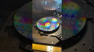
Good point! EUV or extreme ultraviolet lithography is indeed essential for pattern transfer in semiconductor making, especially for nanometer-scale features. These tools are often worth over $100 million! Why do you think optimizing their operation is critical?

Because even a small error can lead to significant defects and loss of yield!
Exactly! The complexity and cost associated with these tools necessitate precise control and optimization. Let's remember the acronym YOD—Yield, Optimization, and Defectivity—as we discuss this section.
Can anyone tell me how the environment might affect these tools?

I guess things like temperature, humidity, and cleanliness in the cleanroom all play a role.
Absolutely right! The operation of these sophisticated machines is sensitive to environmental factors, making real-time monitoring even more crucial.
Equipment Operation Workflow
🔒 Unlock Audio Lesson
Sign up and enroll to listen to this audio lesson

Now, let's take a closer look at the operation workflow of an EUV lithography scanner. What do you think the first step would be?

I imagine it would start with initialization, checking all system parameters?
Exactly! Initialization ensures that the tool checks vacuum levels, optics alignment, and temperature control. After that, the tool loads calibration masks. Can anyone summarize the subsequent steps involved in the recipe execution?
The litho engineer selects process parameters like exposure dose and alignment settings, then adjusts them accordingly.
Right on! After recipe execution, we move to the exposure and stage control, where high-precision stages align the wafer under the EUV beam. Remember to keep the acronym PEP—Process, Exposure, and Post-Processing—in mind.
Real-Time Monitoring & Control Systems
🔒 Unlock Audio Lesson
Sign up and enroll to listen to this audio lesson
Let’s now talk about equipment control and monitoring systems. Does anyone know what Process Control Systems (PCS) are used for?
It manages process parameters like gases and temperature, right?
Correct! PCS ensures that everything is within optimal working conditions. Why might Statistical Process Control (SPC) be necessary?
I think SPC is used to detect process drifts in real-time, which could indicate that something is going wrong.
Great observation! Continuous monitoring helps us catch any issues before they result in yield loss. Remember the acronym PC-MAP—Process Control, Monitoring, and Automation Problems—as a way to link these terms!
Optimization Techniques
🔒 Unlock Audio Lesson
Sign up and enroll to listen to this audio lesson
Now let's explore optimization techniques such as recipe tuning. Can someone explain what this involves?
Recipe tuning is about adjusting process parameters to meet target specifications, usually requiring some experiments.
That's spot on! It might also involve Design of Experiments (DOE) to systematically fine-tune these parameters. What about Run-to-Run control?
That’s where feedback from previous processes is used to enhance the next batch, isn't it?
Exactly! This technique can significantly improve efficiency and yield. Remember the acronym RTE—Run-to-Run Enhancements—when thinking of iterative improvements.
Conclusion and Summarization
🔒 Unlock Audio Lesson
Sign up and enroll to listen to this audio lesson
To wrap up, what is the main takeaway regarding the operation of semiconductor manufacturing equipment?
It's not just about having advanced tools; we need to optimize their operations to maintain high yield.
And monitoring systems are key in helping us identify faults or drifts in performance.
Exactly right! Continuous optimization combined with real-time diagnostics is vital to minimizing defects and ensuring consistent performance. Don’t forget the YOD acronym we discussed earlier!
Introduction & Overview
Read summaries of the section's main ideas at different levels of detail.
Quick Overview
Standard
The section highlights the importance of optimizing the operation of expensive semiconductor manufacturing equipment by explaining key tools, control strategies, and real-time monitoring techniques. It addresses the complexities and operational workflows involved in achieving high yields and minimizing defects in modern fabs.
Detailed
Operation and Optimization of State-of-the-Art Manufacturing Equipment
The operation of advanced semiconductor manufacturing equipment is crucial for achieving high yield and low defectivity when fabricating nanometer-scale features. Semiconductor manufacturing tools, often worth over $100 million, require precise control under stringent environmental conditions. This section explores the principles of operation for key manufacturing tools such as lithography scanners and etchers, as well as the comprehensive workflow involved in their operation. It also elaborates on equipment control and monitoring systems designed to manage process parameters dynamically in real time, ensuring optimal performance.
Key techniques for the optimization of these tools are introduced, including recipe tuning, run-to-run control, predictive maintenance, and chamber matching. Combined with advanced algorithms and data analytics, these techniques contribute to maintaining the integrity and efficiency of manufacturing processes. In essence, operating these state-of-the-art tools demands not only technical knowledge but also a strategic approach to continuous improvement.
Youtube Videos
Audio Book
Dive deep into the subject with an immersive audiobook experience.
Introduction to Semiconductor Manufacturing
Chapter 1 of 3
🔒 Unlock Audio Chapter
Sign up and enroll to access the full audio experience
Chapter Content
Modern semiconductor fabs rely on highly advanced, multi-million-dollar equipment to fabricate nanometer-scale features. The success of a fabrication process depends not only on having state-of-the-art tools but also on optimizing their operation to achieve high yield, low defectivity, and consistent performance. This chapter explores:
● The operation principles of key manufacturing tools.
● Equipment control strategies.
● Techniques for monitoring and optimizing performance in real time.
Detailed Explanation
In modern semiconductor manufacturing, factories use incredibly sophisticated equipment that costs millions of dollars to create very small, precise features on chips. The ability to produce these chips effectively relies not only on having the best tools but also on managing those tools well to ensure they work reliably and produce a lot of good quality products with minimal errors. This chapter will discuss how these tools operate, how they are controlled during manufacturing processes, and how we can continuously monitor and improve their performance.
Examples & Analogies
Think of a high-end restaurant where chefs use the finest ingredients and equipment. If the kitchen is poorly managed or if the chefs don’t optimally use their tools (like knives and pots), the food may not turn out well. Similarly, in semiconductor fabrication, having advanced machines isn’t enough; they must be operated and managed expertly to create great products.
Challenges in Semiconductor Equipment
Chapter 2 of 3
🔒 Unlock Audio Chapter
Sign up and enroll to access the full audio experience
Chapter Content
Semiconductor equipment is:
● Extremely expensive (often >$100M per tool).
● Highly complex, involving vacuum, plasma, lasers, robotics, and advanced sensors.
● Sensitive to environmental factors and process parameters. To ensure high-volume manufacturing success, tools must be operated:
● With tight process windows,
● Under cleanroom constraints, and
● With real-time diagnostics and optimization algorithms.
Detailed Explanation
Semiconductor tools are very costly, often costing more than $100 million each, and they operate using technologies that are incredibly intricate. These tools have to deal with various conditions like vacuum pressure and temperature, and they need to function perfectly to avoid errors. Because of this complexity, operating these machines requires exact standards, known as 'tight process windows,' and they must be kept in cleanrooms free of dust and contaminants. Moreover, real-time monitoring systems are essential to instantly detect and address any issues that arise during the manufacturing process.
Examples & Analogies
Consider a high-performance sports car. It’s expensive, has many complex systems, and requires specific conditions for optimal performance. If the car isn’t maintained properly or if it's driven under the wrong conditions, it won’t perform well. In the same way, semiconductor equipment must be finely tuned and monitored to ensure it functions properly and meets production goals.
Overview of Key Equipment Categories
Chapter 3 of 3
🔒 Unlock Audio Chapter
Sign up and enroll to access the full audio experience
Chapter Content
Category Equipment Function
Lithography DUV, EUV Scanners Pattern transfer
Etching RIE, ICP Etchers Anisotropic material removal
Deposition CVD, PVD, ALD Chambers Thin film formation
Planarization CMP Polishers Surface flattening
Ion Implantation Ion Implanters Doping silicon with desired impurities
Metrology CD-SEM, AFM, Critical dimension and profile Scatterometers inspection
Wafer Handling/Robotics Arms Transport Wafer transfer with no human contact
Detailed Explanation
There are several categories of equipment used in semiconductor manufacturing, each fulfilling a specific role. Lithography tools such as DUV and EUV scanners are responsible for transferring patterns to silicon wafers. Etching tools like RIE and ICP etchers remove material in a controlled manner. Deposition equipment creates thin films on the wafer surface, and planarization tools ensure the surface is smooth. Ion implanting introduces impurities to modify the electrical properties of silicon. Measurements and inspections are done using metrology tools to ensure quality, and robotic systems manage wafer handling to minimize human error.
Examples & Analogies
Imagine a bakery where each type of tool fulfills a unique purpose—mixers for dough, ovens for baking, and icing tools for decoration. Just as each tool in the bakery is essential for creating the final product, each piece of equipment in semiconductor manufacturing plays a unique role in creating functional microchips.
Key Concepts
-
Precision engineering: Essential for the accuracy and performance of semiconductor tools.
-
Optimization strategies: Critical for maintaining yield and minimizing defects throughout the manufacturing process.
-
Real-time monitoring: Necessary for identifying and correcting process deviations promptly.
Examples & Applications
Using recipe tuning to improve the yield of a particular wafer batch by adjusting exposure parameters based on previous data.
Implementing SPC to maintain temperature consistency in wafer processing, which helps in minimizing defects.
Memory Aids
Interactive tools to help you remember key concepts
Rhymes
In semiconductor fab, clarity is key, keep the tools in line, high yields will be!
Stories
Imagine a chef in a high-tech kitchen, adjusting the recipe based on feedback to make the best dish—this mirrors how engineers fine-tune parameters for optimal semiconductor production.
Memory Tools
Remember PEP for the lithography process: Prepare, Execute, and Post-Process.
Acronyms
Use the acronym YOD (Yield, Optimization, Defectivity) to remember the key focus areas of semiconductor operations.
Flash Cards
Glossary
- EUV (Extreme Ultraviolet) Lithography
A cutting-edge lithography technology that uses extreme ultraviolet light to print tiny patterns onto semiconductor wafers.
- Recipe Tuning
The process of adjusting manufacturing parameters to achieve desired specifications and improve production quality.
- Statistical Process Control (SPC)
A method of quality control that uses statistical methods to monitor and control a process.
- RuntoRun (R2R) Control
An optimization method that utilizes data from previous production runs to adjust subsequent ones for improved performance.
- Predictive Maintenance
A maintenance strategy that uses data analysis tools and techniques to predict when equipment failure might occur.
Reference links
Supplementary resources to enhance your learning experience.