
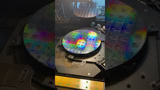
Step 1: Overview of Key Equipment Categories
Interactive Audio Lesson
Listen to a student-teacher conversation explaining the topic in a relatable way.
Lithography Equipment
🔒 Unlock Audio Lesson
Sign up and enroll to listen to this audio lesson

Today, let's explore lithography. Can anyone tell me what type of equipment is involved in lithography?

I think it's the DUV and EUV scanners.
Correct! DUV and EUV scanners are crucial for pattern transfer. What do you think is the importance of pattern transfer in semiconductor manufacturing?

It helps in creating the intricate designs on chips.
Exactly! This is vital for functioning electronic devices. Remember: "Pattern it right, keep the circuits tight!" This mnemonic can help you recall the importance of pattern transfer in lithography.
Etching Process
🔒 Unlock Audio Lesson
Sign up and enroll to listen to this audio lesson

Now, let's dive into etching. Who can name the types of etching equipment?

RIE and ICP etchers?
Right! What does anisotropic material removal mean in this context?

It means that the etching process is directional; it removes material more on one side.
Spot on! Remember: "Etch it right, to avoid a fright!" It reminds you to focus on precision during the etching process.
Deposition Techniques
🔒 Unlock Audio Lesson
Sign up and enroll to listen to this audio lesson
Let’s discuss deposition now. Can anyone give examples of deposition techniques?
CVD, PVD, and ALD!
Great job! What are the primary functions of these deposition methods?
They are used to create thin films on the wafer.
Correct! Remember this acronym: DP for 'Deposit Precisely' to reinforce the idea of precision during deposition.
Wafer Handling and Robotics
🔒 Unlock Audio Lesson
Sign up and enroll to listen to this audio lesson
Lastly, let's examine wafer handling technologies. What do we use to transfer wafers safely?
FOUP load ports and robotic arms!
Yes! These minimize human contact and maintain cleanliness. Why is this cleanliness so important?
To prevent contamination that could affect the semiconductor quality!
Exactly! Think of the rhyme: "Handle with care, or lose a layer!" to remember the significance of clean handling.
Introduction & Overview
Read summaries of the section's main ideas at different levels of detail.
Quick Overview
Standard
The section outlines essential categories of equipment utilized in semiconductor fabrication, including lithography, etching, deposition, planarization, ion implantation, metrology, and wafer handling. Each category is paired with its specific function, illustrating the interdependencies in the manufacturing process.
Detailed
Detailed Overview of Key Equipment Categories
In semiconductor manufacturing, different categories of equipment are employed to ensure precision and efficacy across various stages of fabrication. Below are the main categories and their corresponding functions:
- Lithography - This includes DUV (Deep Ultraviolet) and EUV (Extreme Ultraviolet) scanners which are responsible for pattern transfer onto wafers, enabling the development of intricate circuits that are essential for modern electronics.
- Etching - Equipment such as RIE (Reactive Ion Etching) and ICP (Inductively Coupled Plasma) etchers serve to precisely remove materials from the wafer surface in an anisotropic manner, crucial for defining patterns created during lithography.
- Deposition - Various chambers like CVD (Chemical Vapor Deposition), PVD (Physical Vapor Deposition), and ALD (Atomic Layer Deposition) are used for the formation of thin films on the wafer, which is crucial for semiconductor device functionality.
- Planarization - CMP (Chemical Mechanical Planarization) polishers are used to ensure wafer surface uniformity by eliminating topographical variations, which are vital for subsequent processing steps.
- Ion Implantation - Ion implanters are utilized for doping silicon with selected impurities, an essential process for creating the p-n junctions necessary for semiconductor devices to operate.
- Metrology - Tools such as CD-SEM (Critical Dimension Scanning Electron Microscopy) and AFM (Atomic Force Microscopy) facilitate critical dimension inspection and profile monitoring to ensure the accuracy of fabricated structures.
- Wafer Handling/Robotics - This category includes FOUP (Front Opening Unified Pod) load ports and robotic arms, which aid in the seamless transfer of wafers while minimizing human contact, essential for maintaining cleanroom standards.
Understanding these categories is critical as it highlights the sophisticated and interconnected nature of semiconductor fabrication technologies.
Youtube Videos
Audio Book
Dive deep into the subject with an immersive audiobook experience.
Lithography Equipment
Chapter 1 of 7
🔒 Unlock Audio Chapter
Sign up and enroll to access the full audio experience
Chapter Content
Lithography
Equipment: DUV, EUV Scanners
Function: Pattern transfer
Detailed Explanation
Lithography is a process in semiconductor manufacturing that transfers patterns onto a substrate. There are two main types of lithography equipment: DUV (Deep Ultraviolet) and EUV (Extreme Ultraviolet) scanners. These tools use light to project these patterns onto layers of photoresist material coated on wafers, creating intricate designs needed for chips.
Examples & Analogies
Think of lithography as a high-tech form of stenciling. Just like you might use a stencil to paint a design on a wall, lithography tools shine light through masks (stencils) onto the wafer to create precise patterns for circuits.
Etching Equipment
Chapter 2 of 7
🔒 Unlock Audio Chapter
Sign up and enroll to access the full audio experience
Chapter Content
Etching
Equipment: RIE, ICP Etchers
Function: Anisotropic material removal
Detailed Explanation
Etching is the process of selectively removing material from the wafer to create specific features. RIE (Reactive Ion Etching) and ICP (Inductively Coupled Plasma) etchers are commonly used for this purpose. Anisotropic etching means that the material is removed at different rates depending on the direction—allowing for vertical sidewalls in the features.
Examples & Analogies
Consider etching like carving a statue from a block of stone. You focus your energy in specific areas to carve away more material, creating the desired shape while leaving other parts intact.
Deposition Equipment
Chapter 3 of 7
🔒 Unlock Audio Chapter
Sign up and enroll to access the full audio experience
Chapter Content
Deposition
Equipment: CVD, PVD, ALD Chambers
Function: Thin film formation
Detailed Explanation
Deposition processes are critical in creating thin layers of material on the wafer. CVD (Chemical Vapor Deposition), PVD (Physical Vapor Deposition), and ALD (Atomic Layer Deposition) are methods used to achieve this. These processes enable layers to be formed uniformly across varying surface features.
Examples & Analogies
Imagine coating a cupcake with frosting. Deposition processes are like applying a smooth, even layer of frosting over the entire cupcake, ensuring that every part is covered appropriately, regardless of its shape.
Planarization Equipment
Chapter 4 of 7
🔒 Unlock Audio Chapter
Sign up and enroll to access the full audio experience
Chapter Content
Planarization
Equipment: CMP Polishers
Function: Surface flattening
Detailed Explanation
Chemical Mechanical Planarization (CMP) is a technique used to flatten the surface of the wafer after deposition. CMP polishers use a combination of chemical and mechanical forces to achieve a smooth and even surface, which is crucial for subsequent processing steps.
Examples & Analogies
Think of CMP like polishing a table. Just as you might sand and polish a wooden table to make it smooth and even, CMP processes ensure that the wafer surface is flat enough for the next layers or features.
Ion Implantation Equipment
Chapter 5 of 7
🔒 Unlock Audio Chapter
Sign up and enroll to access the full audio experience
Chapter Content
Ion Implantation
Equipment: Ion Implanters
Function: Doping silicon with desired impurities
Detailed Explanation
Ion implantation involves embedding ions into the silicon substrate to modify its electrical properties, which is critical for creating p-type and n-type semiconductors. Ion implanters accelerate ions into the wafer at specific energies to achieve the desired doping concentration and depth.
Examples & Analogies
You can think of this process as planting seeds in a garden. Just as the depth and spacing of seeds can affect how plants grow, the positioning of ions in silicon can significantly influence the electrical behavior of the semiconductor.
Metrology Equipment
Chapter 6 of 7
🔒 Unlock Audio Chapter
Sign up and enroll to access the full audio experience
Chapter Content
Metrology
Equipment: CD-SEM, AFM, Scatterometers
Function: Critical dimension and profile inspection
Detailed Explanation
Metrology is vital in semiconductor manufacturing as it involves measuring and inspecting the critical dimensions and profile of features on the wafer. Tools like CD-Scanning Electron Microscopes (CD-SEM), Atomic Force Microscopes (AFM), and scatterometers are used to ensure that the dimensions are within specified tolerances.
Examples & Analogies
Think of metrology as taking measurements while baking. Just like measuring flour and sugar ensures you have the right ingredients in the right amounts for baking a cake, metrology ensures that the semiconductor patterns are perfectly sized and shaped for functionality.
Wafer Handling Equipment
Chapter 7 of 7
🔒 Unlock Audio Chapter
Sign up and enroll to access the full audio experience
Chapter Content
Wafer Handling/Robotics
Equipment: FOUP Load Ports, Transport, Robotics Arms
Function: Wafer transfer with no human contact
Detailed Explanation
Wafer handling systems are essential in semiconductor fabs to automate the transfer of wafers between different processing tools without human contact. Equipment like FOUP (Front Opening Unified Pod) load ports and robotic arms ensure that wafers are transported safely and efficiently, reducing contamination risks.
Examples & Analogies
Consider wafer handling like a conveyor belt in a restaurant kitchen. The belt automatically moves dishes from one workstation to another, allowing cooks to focus on their tasks without worrying about spilling or contaminating the food.
Key Concepts
-
Lithography Equipment: Essential for pattern transfer in semiconductor manufacturing.
-
Etching Process: Allows for precise material removal to define structures.
-
Deposition Techniques: Used for forming thin films, integral to semiconductor devices.
-
Planarization: Ensures uniform surface features for subsequent processing.
-
Ion Implantation: Dopes silicon to modify electrical properties.
-
Metrology: Crucial for measuring features and ensuring specification compliance.
-
Wafer Handling: Important for clean and efficient transport of wafers.
Examples & Applications
An EUV scanner that transfers patterns onto silicon wafers, enabling advanced circuit designs.
An etching tool that uses plasma to remove silicon dioxide selectively, defining intricate pathways on a chip.
A CVD chamber that creates a thin layer of silicon nitride on a wafer as part of the isolation process.
Memory Aids
Interactive tools to help you remember key concepts
Rhymes
To etch it right, laser beams must dance, to ensure the patterns have every chance!
Stories
Imagine a tiny workshop where brave wafers are sent off into the wild world of electronics, armed with patterns drawn by DUV scanners.
Memory Tools
Remember L.E.D.M.M.W: Lithography, Etching, Deposition, Metrology, and Wafer handling to cover the key equipment categories.
Acronyms
E.L.P.M
Equipment. Lithography
Planarization
Metrology to recap the key categories quickly.
Flash Cards
Glossary
- Lithography
A process in semiconductor manufacturing used for pattern transfer onto wafers using light.
- Etching
The process of removing material from the wafer surface to create desired patterns.
- Deposition
Techniques used to add thin films of material onto wafers.
- Planarization
A process that flattens the wafer surface to ensure uniform thickness across the wafer.
- Ion Implantation
A technique used to introduce impurities into silicon to modify its electrical properties.
- Metrology
The measurement science concerned with measuring the physical properties of objects, essential in inspection stages.
- Wafer Handling
The process of transferring wafers within a manufacturing environment to ensure integrity and cleanliness.
Reference links
Supplementary resources to enhance your learning experience.