
Step 2: Equipment Operation Workflow
Interactive Audio Lesson
Listen to a student-teacher conversation explaining the topic in a relatable way.
Initialization of Equipment
🔒 Unlock Audio Lesson
Sign up and enroll to listen to this audio lesson

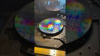
Today, we are going to explore the initialization process of equipment like the EUV Lithography Scanner. Can anyone tell me why initialization is so important?

Is it to make sure everything is set up correctly before starting?
Exactly! Initialization checks the vacuum, optics alignment, and temperature control. This ensures that the equipment is ready to operate without errors.

What happens if any of those checks fail?
Great question! If these checks fail, it could lead to defective wafers, which costs time and money for the fabrication process. Remember the acronym 'VOT'—Vacuum, Optics, Temperature—as key factors in initialization!
Recipe Execution
🔒 Unlock Audio Lesson
Sign up and enroll to listen to this audio lesson

After initialization, the next step is recipe execution. Can someone tell me what a process recipe is?

Is it a set of instructions for how to process the wafer?
Exactly! The litho engineer chooses parameters like exposure dose and focus tailored to the specific layer. It's essential for achieving the desired pattern sizes.

How are those parameters set?
They are adjusted based on the specifications required for the product. A tip—just remember the 'D-F-A' Framework—Dose, Focus, and Alignment for easy recall of key parameters!
Exposure & Stage Control
🔒 Unlock Audio Lesson
Sign up and enroll to listen to this audio lesson
Now, let’s discuss exposure and stage control. Why do you think precision is critical at this stage?
It’s because any misalignment could ruin the wafer pattern, right?
Absolutely! High-precision stages are used to align the wafer, and real-time feedback ensures nanometer-level accuracy. Remember it as 'Aligned Precision for Success'!
What tools help achieve that accuracy?
Great question! Sensors and control algorithms constantly make adjustments for precise positioning.
Post-Processing
🔒 Unlock Audio Lesson
Sign up and enroll to listen to this audio lesson
The last step is post-processing. What should happen after a wafer is exposed?
It needs to be transferred to the next tool, right?
Yes! It goes to post-exposure bake or development tool. Data is also collected during this phase for overlay accuracy. Think of it as 'Process, Analyze, Verify'!
How do we ensure the results are reliable?
By accumulating data continuously during each manufacturing run, we can ensure quality control and precision in the process.
Introduction & Overview
Read summaries of the section's main ideas at different levels of detail.
Quick Overview
Standard
The section provides a step-by-step overview of the operational workflows for semiconductor manufacturing equipment like EUV lithography scanners, detailing processes from initialization and recipe execution to exposure and post-processing, emphasizing the significance of precision and real-time control for successful fabrication.
Detailed
Detailed Summary
This section extensively covers the operational workflow of semiconductor equipment, with a particular focus on an EUV Lithography Scanner. The workflow consists of four main steps:
- Initialization: This first step involves a series of crucial checks including vacuum conditions, optics alignment, and temperature control. The system also loads calibration masks and wafers which are critical for the subsequent processes.
- Recipe Execution: In this step, the lithography engineer selects an appropriate process recipe. This includes setting parameters such as exposure dose, focus, and alignment tailored for specific layers and pattern sizes. The accuracy of these parameters is vital to the outcome of the lithography process.
- Exposure & Stage Control: This step relies on high-precision stages that ensure the wafer aligns correctly under the EUV beam. Real-time feedback mechanisms are employed to maintain nanometer-level accuracy, which is essential for the intricate patterns required in semiconductor fabrication.
- Post-Processing: After exposure, the wafer is transferred to post-exposure bake or development tools. During this phase, data is collected to evaluate overlay accuracy and critical dimensions uniformity.
In conclusion, the outlined workflow is fundamental for the operation of advanced semiconductor manufacturing tools, underscoring the need for precision engineering and real-time diagnostics to ensure optimum performance.
Youtube Videos

Audio Book
Dive deep into the subject with an immersive audiobook experience.
Initialization
Chapter 1 of 4
🔒 Unlock Audio Chapter
Sign up and enroll to access the full audio experience
Chapter Content
• Initialization
- Tool checks vacuum, optics alignment, temperature control.
- System loads calibration masks and wafers.
Detailed Explanation
In the initialization phase, the EUV Lithography Scanner performs several important checks to ensure everything is ready for operation. These checks include verifying that the vacuum system is functioning correctly, aligning the optical components properly, and maintaining the necessary temperature. Once these checks are completed successfully, the scanner loads calibration masks and wafers, which are essential for the exposure process.
Examples & Analogies
Think of this like preparing an advanced coffee machine before making coffee. Just as you would ensure the water tank is filled, the coffee grounds are correctly placed, and the machine is warmed up, the scanner undergoes its checks to ensure it’s ready to produce high-quality results.
Recipe Execution
Chapter 2 of 4
🔒 Unlock Audio Chapter
Sign up and enroll to access the full audio experience
Chapter Content
• Recipe Execution
- Litho engineer selects a process “recipe” (exposure dose, focus, alignment).
- Parameters adjusted for specific layer and pattern size.
Detailed Explanation
During recipe execution, a lithography engineer selects a specific 'recipe' that contains all the parameters needed for the lithographic process. This includes critical factors like exposure dose (the amount of light the wafer is exposed to), focus (how sharply the image is projected), and alignment (how well the layers fit together). The engineer must adjust these parameters based on the specific layer being processed and the desired size of the patterns.
Examples & Analogies
It’s akin to a chef selecting a specific recipe for a dish. Depending on what they're cooking — say a cake or a lasagna — the chef will choose different ingredients and cooking times, much like the engineer adjusts the parameters for each unique layer and design.
Exposure & Stage Control
Chapter 3 of 4
🔒 Unlock Audio Chapter
Sign up and enroll to access the full audio experience
Chapter Content
• Exposure & Stage Control
- High-precision stages align the wafer under the EUV beam.
- Real-time feedback ensures nanometer-level accuracy.
Detailed Explanation
In this stage, the wafer is precisely aligned under the Extreme Ultraviolet (EUV) light beam using high-precision stages. These stages can make tiny adjustments to ensure that the exposure of the wafer happens with nanometer-level accuracy. Additionally, the system uses real-time feedback mechanisms to monitor the process and make adjustments on the fly to maintain this precision throughout the exposure.
Examples & Analogies
Imagine a professional photographer taking a photo. They must keep the camera perfectly steady, and any slight shift can cause a blur. Similarly, the high-precision stages in the scanner must align the wafer with perfect accuracy to ensure clear and precise patterns are formed.
Post-Processing
Chapter 4 of 4
🔒 Unlock Audio Chapter
Sign up and enroll to access the full audio experience
Chapter Content
• Post-Processing
- Wafer is transferred to post-exposure bake or development tool.
- Data is collected for overlay accuracy and CD uniformity.
Detailed Explanation
After exposure, the wafer is moved to a post-processing stage, which can include a baking process or development in a tool that further develops the patterns just created. During this stage, data is collected to evaluate how accurately the layers are overlaid and to check the critical dimensions (CD) for uniformity across the wafer.
Examples & Analogies
This step is similar to baking cookies after cutting them into shape. Once out of the oven, you check to ensure they are the right size and shape. In semiconductor processing, this ensures the patterns are consistent and accurate after exposure.
Key Concepts
-
Initialization: A critical step to prepare equipment for operation ensuring accurate performance.
-
Process Recipe: A combination of parameters that engineers use to control the fabrication process specifically.
-
Real-time Feedback: Mechanisms that allow for immediate adjustments during exposure stage for precision.
-
Post-Processing: The process that happens after initial exposure to verify output quality.
Examples & Applications
During initialization, if the vacuum check fails, the equipment cannot proceed, indicating potential risks.
In recipe execution, adjusting the exposure dose affects how effectively a particular photoresist is used during lithography.
Memory Aids
Interactive tools to help you remember key concepts
Rhymes
Before we start and play the game, check the vacuum, optics, and name the aim!
Stories
Imagine a chef preparing a meal; first, they need the right ingredients and utensils prepped. In semiconductor fabrication, initializing tools is just as necessary to ensure the process creates a masterpiece!
Memory Tools
Remember 'VOT' for initialization checks - Vacuum, Optics, Temp!
Acronyms
D-F-A - Dose, Focus, and Alignment for recipe execution!
Flash Cards
Glossary
- Initialization
The process of checking and preparing equipment for operation.
- Process Recipe
A set of parameters and instructions used for the fabrication of semiconductor layers.
- EUV Lithography
A type of lithography that uses extreme ultraviolet light for patterning in semiconductor fabrication.
- Alignment
The process of positioning components with precision to ensure accurate manufacturing.
- PostProcessing
Further steps taken after the initial exposure to ensure the design is correctly formed on the wafer.
Reference links
Supplementary resources to enhance your learning experience.