
Common Emitter Amplifier (Contd.)
Enroll to start learning
You’ve not yet enrolled in this course. Please enroll for free to listen to audio lessons, classroom podcasts and take practice test.
Interactive Audio Lesson
Listen to a student-teacher conversation explaining the topic in a relatable way.
Specifications for Common Emitter Amplifier
🔒 Unlock Audio Lesson
Sign up and enroll to listen to this audio lesson

Can anyone tell me what initial specifications we typically consider when designing a common emitter amplifier?

We need to know the supply voltage, the type of BJT, and the beta value.
Great! These are crucial – the supply voltage sets our limits, while understanding the BJT type helps determine its characteristics. Remember, for silicon, we have different parameters than germanium.

How do we determine what resistor values to use?
Good question! The resistor values come from the design requirements. We typically start by calculating the bias resistors and coupling capacitors based on expected gain and output swing.

What is the focus for gain and output swing?
Exactly! The quiescent point should be set in the middle to maximize our swing, which also minimizes distortion.
So, to summarize today, ensure you gather the BJT type and supply voltage details before starting your calculations. This sets the foundation for everything else.
Calculating Gain and Output Swing
🔒 Unlock Audio Lesson
Sign up and enroll to listen to this audio lesson

Let’s dive into how we calculate voltage gain, who can give me the formula?

Is it Av = gm × RC?
Exactly! And remember gm is determined by the quiescent current divided by the thermal voltage. This means we must consider quiescent current values carefully.
How does supply voltage affect output swing?
The output swing is limited by the supply voltage and the saturation points of the transistor. Setting a proper quiescent point allows a good range of swing without distortion.
How do we avoid distortion in the output?
Set your quiescent point in a way that it’s centered in the output voltage range. This lets the signal fluctuate evenly around that point.
To sum up, ensure you account for these limits when designing; they play a significant role in circuit performance.
Power Dissipation and Overall Design Strategy
🔒 Unlock Audio Lesson
Sign up and enroll to listen to this audio lesson
Now, let’s discuss power dissipation. Can anyone define it in this context?
It's the product of voltage and current through the circuit?
Correct! Knowing the quiescent current and the supply voltage helps us compute this effectively. We want to keep dissipation within reasonable limits.
How does this influence our resistor choices?
Great connection! Resistor values have to suit the power limits—choose resistors that can handle the power without overheating or failing.
What about the capacitors? Are there specific guidelines for them?
Definitely! Capacitor values are determined partly by the input resistance and the desired lower cutoff frequency. Typical values might range in microfarads.
In summary, understand your current paths and power needs thoroughly. It’s critical for a reliable design.
Introduction & Overview
Read summaries of the section's main ideas at different levels of detail.
Quick Overview
Standard
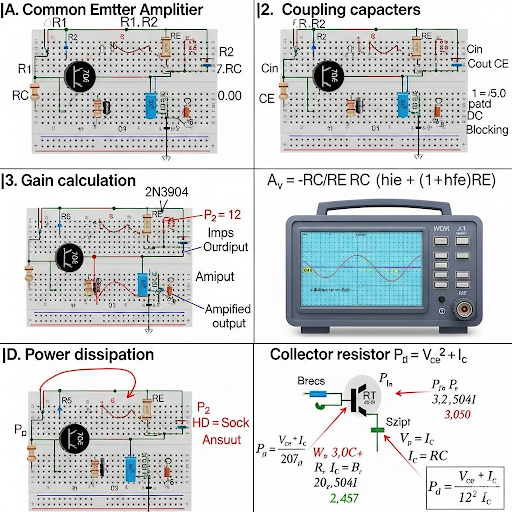
The section discusses the design principles behind the common emitter amplifier, emphasizing how to determine important parameters such as gain, output swing, and power dissipation. It also addresses design strategies applicable when the circuit topology is fixed and outlines the necessary calculations based on given specifications.
Detailed
Common Emitter Amplifier (Contd.)
This section elaborates on the design guidelines for common emitter amplifiers within the context of analog electronic circuits. Starting by summarizing prior discussions, the instructor revisits numerical problems, helping students understand how to analyze circuits and find necessary parameters for designing amplifiers. The key focus areas include:
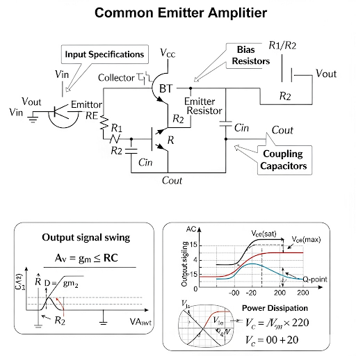
- Input Specifications: Designers typically begin with the supply voltage, type of BJT (silicon or germanium), and transistor beta (β).
- Design Principles: The design task primarily involves determining bias resistors and coupling capacitors (C1 and C2). Guidelines for their selection depend on desired circuit performance metrics, such as gain and output signal swing.
- Gain Calculation: The voltage gain (Av) is calculated as Av = gm × RC, noting that gain is subject to transistor characteristics and supply voltage constraints.
- Output Signal Swing: The section emphasizes achieving a quiescent point that allows for maximum signal swing, setting it at the midpoint to optimize performance while avoiding distortion.
- Power Dissipation: This includes calculations for quiescent current and overall power consumption, which affects the voltage drop across resistors, ultimately influencing design parameters like the choice of RC.
Through numerical examples and problem-solving strategies, students glean insight into designing common emitter amplifiers for a range of applications.
Youtube Videos

Audio Book
Dive deep into the subject with an immersive audiobook experience.
Introduction to Design Guidelines
Chapter 1 of 7
🔒 Unlock Audio Chapter
Sign up and enroll to access the full audio experience
Chapter Content
Hello, so now so, welcome back to this NPTEL online course on Analog Electronic Circuits. This is of course, it is we are having this course for maybe last 2 to 3 weeks, it is continuation of that topic of Common Emitter Amplifier. We have discussed about the theoretical aspect and some of the numerical examples, and in the previous class we could not complete the numerical problems all. So, today we are discussing some more numerical problems.
Detailed Explanation
The instructor begins by welcoming students back to the course, emphasizing that this lesson continues from previous discussions on the Common Emitter Amplifier (CEA). In prior classes, theoretical aspects and numerical problems were covered, although not all problems were completed previously. This session is intended to expand on previous examples and focus on designing the CEA based on provided requirements.
Examples & Analogies
Imagine you are working on a complex recipe where some steps from previous cooking sessions were left unfinished. Each time you come back, you review and expand on your understanding, much like building upon the previous lessons in your electronics course.
Understanding Design Requirements
Chapter 2 of 7
🔒 Unlock Audio Chapter
Sign up and enroll to access the full audio experience
Chapter Content
So, today what will be doing is that in case if we have to design one common emitter amplifier for a given requirement, then how do you proceed and what may be the design guidelines we need to follow.
Detailed Explanation
In this part of the discussion, the instructor outlines the essential steps needed to design a common emitter amplifier based on specific requirements. This includes understanding the key parameters needed, such as supply voltage and transistor type, which will influence the design decisions.
Examples & Analogies
Designing an amplifier is like building a custom piece of furniture. You start with understanding the space (requirements) you have to work with, materials (components required), and the desired style (design guidelines) before you start building.
Key Design Parameters
Chapter 3 of 7
🔒 Unlock Audio Chapter
Sign up and enroll to access the full audio experience
Chapter Content
And, so, we are going to discuss detail about the design guidelines of common emitter amplifier. And, in case if the topology is fixed and if it is decided to be fixed by us topology. And, then how do you proceed first thing is that we are assuming that these informations are available particularly the supply voltage it is given to us.
Detailed Explanation
Here, the instructor highlights that the design guidelines will be based on several critical parameters. An important factor is the topology of the amplifier, which must be predetermined. The supply voltage is one of the primary specifications provided, helping to dictate the subsequent design decisions.
Examples & Analogies
Consider cooking with a recipe that specifies the oven temperature (supply voltage). Just as the cooking process will change based on whether the oven is set to 350°F or 450°F, the amplifier's behavior will depend on the supply voltage you choose.
Current and Power Dissipation
Chapter 4 of 7
🔒 Unlock Audio Chapter
Sign up and enroll to access the full audio experience
Chapter Content
We can say that in the power dissipation it is essentially means that, the value of the collector current. And, then the additional information it may be required is that what may be the input resistance of the circuit, small signal or large signal input resistance, then output resistance of the amplifier.
Detailed Explanation
In this section, the importance of understanding power dissipation is emphasized. Power dissipation primarily relates to the current flowing through the transistor. Additional parameters to consider include the input and output resistance of the circuit, which affect performance characteristics such as gain and overall efficiency.
Examples & Analogies
Imagine your home’s electrical system. Just like knowing how much current (power) your appliances draw can prevent overload on your circuit (power dissipation), understanding the currents in the amplifier design prevents overheating and ensures efficient operation.
Voltage Gain and Output Swing
Chapter 5 of 7
🔒 Unlock Audio Chapter
Sign up and enroll to access the full audio experience
Chapter Content
So, as I said that this is what we are from in fact, we already have covered significant part of the numerical examples. And, particularly the operating point and then the and it is stability and then finding performance matrices.
Detailed Explanation
This part discusses how the voltage gain of the common emitter amplifier and the output swing are related to the design. Understanding how to maintain stability and a favorable operating point ensures the amplifier can achieve the desired performance without distortion.
Examples & Analogies
Think of a see-saw in a playground. If you want it to tilt in a balanced way (operating point), you need to position the riders correctly (gain vs. swing). If everyone is too heavy on one side, it won’t function as intended.
Calculating Design Components
Chapter 6 of 7
🔒 Unlock Audio Chapter
Sign up and enroll to access the full audio experience
Chapter Content
So, I should say this is the upper limit of the voltage gain giving importance to the output swing. And, in this case if I say that V is very small and then we can say that upper limit of the voltage gains, we can practically you can say this is .
Detailed Explanation
Here the instructor explains how to determine the upper limit of voltage gain by considering various constraints such as supply voltage and output swing. By making appropriate calculations, one can optimize the design for better performance outcomes.
Examples & Analogies
This is similar to tuning a musical instrument. The maximum volume (gain) you can get from the instrument depends on how tightly you tune each string (parameters). If one is too loose, it affects the entire sound output.
Finalizing Component Values
Chapter 7 of 7
🔒 Unlock Audio Chapter
Sign up and enroll to access the full audio experience
Chapter Content
So, once we decide that the output swing we want it should be 5 V this is a 2 V, then naturally the drop across this resistance it is also getting fixed, because this is the we like to say this operating point almost at the middle.
Detailed Explanation
In this final chunk, the instructor provides guidance on how to finalize component values to ensure that the amplifier meets the predefined output swing requirements. Decisions regarding resistor values directly influence the voltage drop and the overall gain.
Examples & Analogies
This can be likened to planning a road trip. You must consider how much fuel (voltage swing) you need to reach each destination. Adjusting one stop (resistor value) affects the entire journey (circuit performance).
Key Concepts
-
Gain: The ratio of output voltage change to input voltage change in an amplifier.
-
Power Dissipation: The total power converted into heat within the amplifier circuit.
-
Quiescent Point: The DC voltage at which the amplifier operates in idle conditions.
-
Output Swing: The maximum possible voltage range of the output signal before clipping occurs.
Examples & Applications
If a common emitter amplifier is designed with a supply voltage of 12V and a quiescent current of 1mA, the expected power dissipation can be calculated as P = VCC * IC = 12V * 1mA = 12mW.
For a desired gain of 100 and if we have a gm of 0.078 mS, the required collector resistor RC can be calculated as: AC = gm * RC, giving RC = AC/gm = 100/0.078 ms = 1282.05 Ω.
Memory Aids
Interactive tools to help you remember key concepts
Rhymes
In a BJT fair, voltage gain we share, set the quiescent right, for signal's delight.
Stories
Imagine a concert where the singer's voice is weak. The amplifier boosts the voice, ensuring everyone hears it clearly, just like adjusting our quiescent point to maximize output swing.
Memory Tools
To remember the order of steps in designing the circuit: V-D-B-R-C. (V for Voltage Specification, D for Desired Gain, B for Biasing Resistors, R for Resistor Values, C for Circuit Check).
Acronyms
G-P-O for Gain, Power, and Output. Key focus when considering amplifier design.
Flash Cards
Glossary
- Common Emitter Amplifier
A basic amplifier configuration using a BJT where input is applied between base and emitter and output is taken between collector and emitter.
- Gain
The ratio of output voltage to input voltage, often expressed in decibels (dB).
- Quiescent Point
The DC operating point of a transistor amplifier when no signal is applied.
- Saturation
A condition in which the transistor is fully on and cannot increase output current despite increases in input.
- Power Dissipation
The conversion of electrical energy into heat within the circuit components.
Reference links
Supplementary resources to enhance your learning experience.