
Self-Bias Common Emitter Amplifier
Enroll to start learning
You’ve not yet enrolled in this course. Please enroll for free to listen to audio lessons, classroom podcasts and take practice test.
Interactive Audio Lesson
Listen to a student-teacher conversation explaining the topic in a relatable way.
Introduction to Amplifier Design
🔒 Unlock Audio Lesson
Sign up and enroll to listen to this audio lesson

To start, why do you think we need specific design guidelines for common emitter amplifiers?

Because they affect how well the amplifier will perform?
Exactly! The design guidelines help us optimize performance, particularly gain and output swings. Remember, we want our amplifier to do its job without distortion.

What about the power dissipation aspect?
Great point! Power dissipation depends mainly on the quiescent current flowing through your device. Balancing current and voltage is essential.
Understanding Parameters
🔒 Unlock Audio Lesson
Sign up and enroll to listen to this audio lesson

Can anyone name critical parameters we need to know before we design a common emitter amplifier?

Supply voltage and the type of BJT?
Right! Those are the basics. We also need to understand the β of the transistor for accurate calculations.

What’s the best way to approach this design once we have those values?
Let's focus first on selecting the values for biasing resistors, then we can determine the capacitors based on those resistances and the desired frequency response.
Calculating the Gain
🔒 Unlock Audio Lesson
Sign up and enroll to listen to this audio lesson
To calculate voltage gain, which formula can we use?
Isn't it based on gm and RC?
Yes! The voltage gain Av is given by Av = gm × RC. Can someone explain what each component represents?
gm is the transconductance and RC is the collector resistance, right?
Perfect! Now, remember, gm is also related to the quiescent current. So, as we choose RC, we must consider the input signal and the desired output swing.
Output Swing and Biasing
🔒 Unlock Audio Lesson
Sign up and enroll to listen to this audio lesson
What do we mean by output swing in amplifiers?
It’s the range of voltages the amplifier can output without distortion?
Exactly! Setting a proper quiescent point ensures symmetrical output swing. What factors do you think affect this output swing the most?
The supply voltage and how we set the bias resistors?
Right! The first step is to set our quiescent point at half of the supply voltage, allowing good performance on both sides.
Practical Examples
🔒 Unlock Audio Lesson
Sign up and enroll to listen to this audio lesson
Let’s apply our knowledge to a practical scenario. Suppose we need a common emitter amplifier with a supply voltage of 12V. What would be the first step?
Determine the collector and base resistors based on the given specifications!
Exactly! And what if the desired gain was 230, what additional calculations would we perform?
We'd need to ensure the drop across RC is close to VCC to achieve that gain...
Yes! That balance is key. Ensure the quiescent point aligns to maintain output swing too.
Introduction & Overview
Read summaries of the section's main ideas at different levels of detail.
Quick Overview
Standard
The section delves into the design principles underlying self-bias common emitter amplifiers, emphasizing the importance of supply voltage, quiescent current, and other parameters in calculating the amplifier’s gain and output swing. It provides a practical approach to designing the circuit components based on user requirements and explains critical aspects related to power dissipation and frequency response.
Detailed
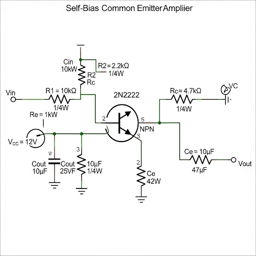
Self-Bias Common Emitter Amplifier
The self-bias common emitter amplifier is a widely used configuration in analog electronics. In this section, we discuss the design guidelines necessary for creating an effective circuit setup. The approach hinges on three core components:
- Supply Voltage: The maximum and minimum voltage must be well understood. The supply voltage is specified by the user and dictates multiple aspects of amplifier performance.
- BJT Characteristics: The type of BJT (silicon or germanium) influences its operating parameters, including threshold voltages and current gain (β). This knowledge is crucial for setting biasing resistors and capacitors accurately.
- Power Considerations: Effective design balances the quiescent current and power dissipation. We explore how to select resistor values that optimize both gain and output swings without causing distortion, leading to better efficiency and performance.
The section transitions into a more practical modality, addressing multiple aspects like using feedback loops, calculating load lines, and ensuring output swings are appropriate given the circuit design. We also cover how to utilize numerical methods for effective circuit analysis and ensure reliable performance metrics.
Youtube Videos

Audio Book
Dive deep into the subject with an immersive audiobook experience.
Introduction to Design Guidelines for Self-Bias Circuit
Chapter 1 of 5
🔒 Unlock Audio Chapter
Sign up and enroll to access the full audio experience
Chapter Content
So, here we do have self-bias and here again we are assuming that these informations are given to us namely, the supply voltage is given to us V it is coming from the data set, BE(on) the β also may be coming from the datasheet or it may be you can use multi meter or by some other means to find the value of β.
Detailed Explanation
The section introduces the design guidelines for a self-bias common emitter amplifier. It specifies that several key parameters are assumed to be provided: the supply voltage (V_CC), the base-emitter on voltage (V_BE(on)), and the transistor's beta (β). These parameters are essential for designing an effective amplifier circuit, as they'll influence the current flow and the overall gain of the amplifier.
Examples & Analogies
Think of this process as preparing a recipe. Before you start cooking, you need to know what ingredients you have. Similarly, before designing an amplifier, you need the essential values such as voltage and current to ensure the final product works as intended.
Understanding Voltage Requirements
Chapter 2 of 5
🔒 Unlock Audio Chapter
Sign up and enroll to access the full audio experience
Chapter Content
Now, compared to the previous circuit they approach it will be similar, but you need to understand that the entire V voltage it is not available for this collector. So, we do have V requirement, V minimum V requirement lower side, in addition to that there is a voltage d c voltage require there.
Detailed Explanation
This chunk explains that not all of the supply voltage (V_CC) is useable for the collector voltage. There are minimum voltage requirements for the emitter (V_E) and for the transistor's saturation voltage (V_CE(sat)). Therefore, the available collector voltage for signal swinging is reduced, based on these minimum voltage requirements.
Examples & Analogies
Imagine trying to fill a glass of water. If the glass has a hole (representing voltage drop requirements), you can't fill it to the top without spilling. Similarly, in a common emitter amplifier, you can't use all of your supply voltage effectively due to these minimum voltage thresholds that must be maintained to prevent distortion.
Impact of Emitter Resistance
Chapter 3 of 5
🔒 Unlock Audio Chapter
Sign up and enroll to access the full audio experience
Chapter Content
Note that while we are connecting the C and if we are applying a signal here the voltage here it will be d c. So, this d c voltage it depends on how much the value of this R we are taking and how much the current emitter current or collector current is flowing through the device.
Detailed Explanation
The section emphasizes the importance of the emitter resistance (R_E) in the circuit design. The DC voltage at the emitter is affected by R_E and the current flowing. A higher emitter resistance results in a higher voltage drop, which reduces the available collector voltage for swings, impacting amplification.
Examples & Analogies
You can think of this concept like a bike ride. The more energy you exert pedaling uphill (higher resistance), the less energy you’ll have available for speed or distance (signal swing). Therefore, finding the right balance is crucial in amplifier design.
Power Dissipation Considerations
Chapter 4 of 5
🔒 Unlock Audio Chapter
Sign up and enroll to access the full audio experience
Chapter Content
Typically whatever the current it will be flowing here I the current base current it will be 2 order magnitude lower and we like to take this current may be in the order of one order magnitude higher than the I.
Detailed Explanation
This section addresses the power dissipation in the circuit. It mentions that the base current (I_B) is much smaller than the collector current (I_C). A sufficiently small base current can help manage power dissipation, but it is also important to ensure that the total power through the circuit remains below safe levels to prevent overheating.
Examples & Analogies
Think of a road trip: if you carry too many heavy bags (too much current), your car (amplifier) can overheat and break down. Keeping the load balanced allows for a smoother ride, just like managing power dissipation helps stabilize circuit operation.
Designing Resistors Based on Emitter Voltage
Chapter 5 of 5
🔒 Unlock Audio Chapter
Sign up and enroll to access the full audio experience
Chapter Content
So, once we decide that the output swing we want it should be 5 V this is a 2 V, then naturally the drop across this resistance R .
Detailed Explanation
After determining the desired output swing, the design focuses on finding corresponding resistor values. The voltage is adjusted according to the required emitter voltage to achieve optimal amplification while ensuring voltage drops at the collector meet operational criteria.
Examples & Analogies
This is like planning a budget for a party: if you want to have a certain amount of fun (output swing), you need to allocate funds (resistances) wisely to different aspects of the party to ensure everything runs smoothly without exceeding your budget.
Key Concepts
-
Supply Voltage: The source voltage provided to the circuit, affecting gain and power dissipation.
-
Biasing Resistors: Resistors used to set the operating point of the transistor for optimal performance.
-
Voltage Gain: The ratio of output voltage to input voltage in an amplifier, critical for determining amplifier performance.
-
Output Swing: The maximum voltage drop that can occur at the output without clipping the signal.
Examples & Applications
If a common emitter amplifier is designed for a supply voltage of 12V and a desired output swing of ±5V, the quiescent point is set to 6V to ensure maximal voltage swing.
For a transistor with β=100, if the collector current is set to 1mA, the base current can be calculated as Ib = Ic/β = 1mA/100 = 0.01mA.
Memory Aids
Interactive tools to help you remember key concepts
Rhymes
For gain we seek and quiescent flow, 12 volts high, lets signals grow.
Stories
Once in a tech lab, a young engineer maximized her amplifier's gain by carefully selecting her quiescent point, ensuring she had the best swing possible. With smart resistor choices, she made the circuit sing, amplifying her signals beautifully.
Memory Tools
GAP - Gain, output swing, and power dissipation are the three pillars of amplifier design.
Acronyms
BAS - Biasing Resistors, Amplifier specs, Supply Voltage are essential for good design.
Flash Cards
Glossary
- Common Emitter Amplifier
A type of amplifier that uses a bipolar junction transistor (BJT) where the input is applied to the emitter and the output is taken from the collector.
- Quiescent Current
The steady-state current flowing through the amplifier when there is no input signal present.
- Transconductance (gm)
A measure of how effectively a transistor can control the output current based on the input voltage.
- Collector Resistance (RC)
The resistance connected to the collector of a transistor which influences the gain of the amplifier.
- Supply Voltage (VCC)
The voltage supplied to the amplifier circuit for its operation.
Reference links
Supplementary resources to enhance your learning experience.