
Power Dissipation and Current
Enroll to start learning
You’ve not yet enrolled in this course. Please enroll for free to listen to audio lessons, classroom podcasts and take practice test.
Interactive Audio Lesson
Listen to a student-teacher conversation explaining the topic in a relatable way.
Introduction to Common Emitter Amplifier Design
🔒 Unlock Audio Lesson
Sign up and enroll to listen to this audio lesson

Welcome to today's session! Today, we will dive into the design of common emitter amplifiers. To begin, what parameters do we need to start designing our amplifier?

Is the supply voltage one of them?
Yes, absolutely! The supply voltage, or Vcc, is essential. Additionally, we need to know whether we're using a silicon or germanium BJT, and the transistor's beta value. Can anyone tell me how we would determine the bias resistors using this information?

Maybe we need to find the quiescent current first?
Exactly! After deciding on these parameters, the next step is to calculate the quiescent current and subsequently set the bias resistors.

What is the significance of the quiescent current?
Great question! The quiescent current affects power dissipation, efficiency, and overall stability. Remember the acronym 'PQE' — Power, Quiescent, Efficiency! This will help us recall its importance.
Calculating Power Dissipation
🔒 Unlock Audio Lesson
Sign up and enroll to listen to this audio lesson

Now, let’s calculate power dissipation. Can anyone remind me how we find it?

Is it by multiplying Vcc and IC?
Correct! The formula is: P_D = Vcc × IC. Why is it critical to understand power dissipation?
Because it affects the thermal stability of the circuit!
Precisely! Remember that insufficient thermal management can lead to failure. Now, what happens if the power dissipation exceeds the wattage rating of the components?
They could overheat and get damaged?
Exactly! It’s crucial to avoid exceeding ratings. To help remember: think of the phrase 'Stay Cool' which stands for managing heat correctly in our circuits.
Understanding Voltage Gain
🔒 Unlock Audio Lesson
Sign up and enroll to listen to this audio lesson
Next, let's discuss voltage gain. Can anyone share how to express the voltage gain of our amplifier?
It's A_v equals g_m multiplied by R_C, right?
Exactly! But also remember the practical considerations, such as output swing. Can anyone explain what output swing is?
It's the range in which the output voltage can vary without distortion.
Right on! A proper output swing maximizes signal integrity. Consider the acronym 'OSG' — Output Swing Gain, it captures the essence of maintaining signal fidelity.
What happens if we ignore the output swing in our calculations?
Ignoring it can lead to clipping or distortion of signals. Always ensure to account for it! Let’s always check the limits based on supply voltage and desired signal amplitude.
Choosing Appropriate Capacitors
🔒 Unlock Audio Lesson
Sign up and enroll to listen to this audio lesson
Finally, let’s delve into selecting coupling capacitors. How do we determine their values?
Don't we need to know the input resistance?
Yes, correct! The input resistance when coupled with capacitors determines the lower cutoff frequency. Let's use the formula for cutoff frequency to find the capacitor values. Who knows the cutoff frequency equation?
It's f_cutoff equals 1 over 2πRinC!
Excellent! Remember the mnemonic 'FRC' for Frequency, Resistance, and Capacitance. Can someone tell me what adjustments can be made if we need to achieve a different cutoff frequency?
We can adjust R or C based on design requirements!
Well done! Always ensure that modifications align with desired performance without causing instability.
Introduction & Overview
Read summaries of the section's main ideas at different levels of detail.
Quick Overview
Standard
In this section, we discuss the essential aspects of designing common emitter amplifiers, including the power dissipation relative to quiescent current, determining gain, and appropriately setting bias resistors and coupling capacitors to meet design specifications. We will outline necessary calculations to ensure the correct performance of the amplifier circuits.
Detailed
Power Dissipation and Current
In the context of designing a common emitter amplifier (CEA), power dissipation and current management are critical factors that dictate the circuit's performance. This section outlines crucial design guidelines that aid in properly configuring a CEA.
Key Points:
- Defining Parameters for Design:
- The fundamental parameters required for designing a CEA include supply voltage (Vcc), type of BJT (silicon or germanium), and the transistor's transfer function (DC).
- Designing involves setting bias resistors and capacitor values based on these parameters to achieve desired performance metrics like gain and output swing.
- Power Dissipation Calculation:
- Power dissipation is primarily determined by the quiescent current flowing through the transistor. It can be calculated using the formula:
$$ P_{D} \approx V_{cc} \times I_{C} $$
Knowing this helps in maintaining thermal stability in the circuit.
- Voltage Gain Determination:
- Voltage gain (Av) of the CEA can be represented as:
$$ A_{v} = g_m imes R_C $$
where g_m is the transconductance and R_C represents the load resistance in the collector. The nature of the output swing is also factored into calculations to avoid significant distortion.
- Biasing and Capacitors:
- Properly setting the values of bias resistors helps stabilize the operating point of the transistor. The time constants associated with coupling capacitors must consider the corresponding input resistance to find the lower cutoff frequency necessary for the circuit operation.
- Design Strategies:
- A systematic approach to design involves a sequence where the voltage gain, power dissipation, and quiescent currents are prioritized, followed by calculating resistor values.
- Adjustments to R_E and coupling capacitor values (C1 and C2) ensure that both DC biasing and AC signal coupling/decoupling meet the performance needs of the circuit.
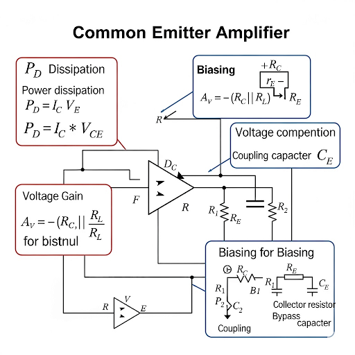
These guidelines provide a structured approach to designing common emitter amplifiers with respect to ensuring optimal performance, stability, and efficiency.
Youtube Videos

Audio Book
Dive deep into the subject with an immersive audiobook experience.
Power Dissipation Basics
Chapter 1 of 4
🔒 Unlock Audio Chapter
Sign up and enroll to access the full audio experience
Chapter Content
So, we can say that power dissipation is essentially defined by how much the quiescent current is flowing through the transistor I_C and I_B. Therefore, we can say that in power dissipation it essentially means the value of the collector current.
Detailed Explanation
Power dissipation in electronic circuits refers to the process during which electrical energy is converted into heat. This heat occurs due to the flow of current, specifically the quiescent current (I_C) in a transistor. In the context of a Common Emitter Amplifier, power dissipation is a crucial aspect because it affects the performance and reliability of the circuit. The collector current (I_C) primarily determines the heat generated in the transistor. If this current is too high, it can lead to overheating and potentially damage the transistor.
Examples & Analogies
Think of power dissipation like a car engine; just as an engine generates heat while running, an electronic component generates heat based on the current flowing through it. If the engine runs too hot without proper cooling, it could fail. Similarly, in electronics, if a transistor dissipates too much power without adequate heat management, it can also fail.
Designing for Current
Chapter 2 of 4
🔒 Unlock Audio Chapter
Sign up and enroll to access the full audio experience
Chapter Content
Based on this power dissipation information, we can find the value of the quiescent current. For that, we can say this power dissipation is approximately equal to V_CC × I_C.
Detailed Explanation
To calculate the required quiescent current (I_C) for a circuit, you typically start with the power dissipation formula. It implies the product of the supply voltage (V_CC) and the current flowing through the collector, which is generally expressed as P = V × I. Rearranging this equation allows you to determine how much current should ideally flow to keep power dissipation within safe limits, thus preventing overheating and ensuring component longevity.
Examples & Analogies
Consider a light bulb powered by a battery. The higher the voltage (like V_CC), the more current it will draw to produce light (like I_C). However, if too much current is drawn, the bulb can blow out due to excess heat (power dissipation). Thus, calculating the right current is essential to prevent such 'blowouts' in a circuit.
Impact of Collector Current on Gain
Chapter 3 of 4
🔒 Unlock Audio Chapter
Sign up and enroll to access the full audio experience
Chapter Content
As I have discussed, if power dissipation allows, we can aim for a voltage drop close to V_CC across the resistor to maximize gain without significant distortion.
Detailed Explanation
In amplifier design, particularly with common emitter amplifiers, optimizing the collector current (I_C) directly affects the gain. The voltage drop across the load resistor (R_C) must be maximized while ensuring it does not cause distortion, which can happen if the output signal swings below V_CE(sat) threshold values. By finding a balance in the current, designers can maximize gain while maintaining signal integrity.
Examples & Analogies
Imagine a water pipe: the pipe can only carry a certain amount of water (current). If we increase the diameter (resistor) too much while trying to push more water (current), it might overflow (distortion). Similar principles apply to electrical signals in amplifiers, where managing the amount of current and ensuring proper resistance can yield the best 'flow' or gain in signal output without distortion.
Overall Design Considerations
Chapter 4 of 4
🔒 Unlock Audio Chapter
Sign up and enroll to access the full audio experience
Chapter Content
Thus, the first thing is that a drop across this resistor can take half of the supply voltage. Then, from power dissipation, we can find what will be the quiescent current.
Detailed Explanation
When designing an amplifier, setting the voltage drop across the load resistor to about half of the supply voltage is a common strategy. This setting helps ensure a balance between gain and output swing. After setting this voltage drop, the quiescent current is derived from the total power dissipation, giving designers a solid foundation for further calculations of biasing and other components in the circuit.
Examples & Analogies
Think of it as a seesaw in a playground: if you want balance (signal integrity), you position the weight (voltage drop) evenly from the center. If one side is heavier, it tilts, representing distortion. Keeping the 'weight' balanced at half the height of the seesaw (supply voltage) allows for optimal functioning of the overall system.
Key Concepts
-
Power Management: A crucial aspect of amplifier design ensuring the circuit operates within temperature limits.
-
Bias Resistors: Components vital for setting the operating point of the circuit.
-
Quiescent Current: The steady-state current critical for evaluating power dissipation and transistor operation.
-
Voltage Gain: Essential for determining amplifier performance and efficiency.
-
Coupling Capacitors: Key in maintaining signal integrity while ensuring DC isolation.
Examples & Applications
If the supply voltage (Vcc) is 12V and the desired quiescent current (IC) is 2mA, the power dissipation would be P_D = 12V * 2mA = 24mW.
To achieve a voltage gain of 100 with a collector resistor of 1kΩ, the transconductance (gm) would need to be 0.1mS, calculated as Av = gm * RC.
Memory Aids
Interactive tools to help you remember key concepts
Rhymes
Gain is a win, check the quiescent twin, adjust with care, let the currents pair.
Stories
Imagine a chef (the circuit) preparing a dish (signal). The ingredients (current/voltage) must be measured perfectly. Too much heat (power dissipation) can spoil the dish.
Memory Tools
PQE - Power, Quiescent, Efficiency: Remember the three essentials of amplifier design.
Acronyms
OSG - Output Swing Gain
Recall the importance of maintaining good output swing for signal integrity.
Flash Cards
Glossary
- Common Emitter Amplifier (CEA)
A type of transistor amplifier that provides significant voltage gain.
- Power Dissipation
The process in which an electronic device dissipates energy as heat.
- Quiescent Current (IC)
The steady-state current flowing through a transistor when no input signal is applied.
- Voltage Gain (Av)
The ratio of output voltage to input voltage in an amplifier.
- Bias Resistors
Resistors used to set the operating point of the transistor in an amplifier.
- Coupling Capacitors
Capacitors that connect two circuit stages while blocking DC signals but allowing AC signals to pass through.
Reference links
Supplementary resources to enhance your learning experience.