
Finding Drain Resistance
Enroll to start learning
You’ve not yet enrolled in this course. Please enroll for free to listen to audio lessons, classroom podcasts and take practice test.
Interactive Audio Lesson
Listen to a student-teacher conversation explaining the topic in a relatable way.
Understanding Bias Resistors
🔒 Unlock Audio Lesson
Sign up and enroll to listen to this audio lesson

Today, we're diving into the critical role of bias resistors in the common source amplifier. Can anyone tell me why biasing is important?

Isn't it to ensure the transistor stays in the saturation region?
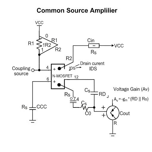
Exactly! If the transistor is not properly biased, it may not amplify the signal correctly. The bias resistors help establish the DC voltages necessary for operation. Now, can someone explain the significance of R1 and R2?

R1 and R2 work together to set the gate voltage, which ultimately determines the drain current.
Correct! And remember, we can express the relationship of these resistors with the formula: VGS = Vdd * R2 / (R1 + R2). Keep this in mind as we progress!

Can we use any values for R1 and R2, or do they need to be specific?
Great question! They need to be chosen based on the current and characteristics of the transistor to ensure good performance. Let's summarize here: bias resistors control the gate voltage and influence the DC operating point.
Calculating the Output Voltage Swing
🔒 Unlock Audio Lesson
Sign up and enroll to listen to this audio lesson

Next up is the output voltage swing. Why do you think it's important to have a good range of output swing?

A greater swing means the amplifier can handle larger signals without distortion.
Exactly! Positioning the DC voltage at the middle of the two extremes—(VGS - Vth) and Vdd—gives us the potential for equal positive and negative swings. Can anyone express this condition mathematically?
Wouldn't it be: VDS = (Vdd - (VGS - Vth)) / 2?
Almost! We ensure that VDS is at the midpoint, which gives us maximum swing. Remember, the goal is centered output voltage!
What happens if the operating point is skewed?
Good catch! Skewing the point reduces one side's swing, leading to distortion. Always strive for balance!
So, it's really about maximizing that output range.
Exactly! To summarize: an optimal output swing is vital for signal integrity and should be equidistant in both directions from the DC operating point.
Finding Drain Resistance
🔒 Unlock Audio Lesson
Sign up and enroll to listen to this audio lesson
Now, let’s explore how we find the drain resistance, RD. Why is RD important?
It helps set the output voltage level and allows the amplifier to maintain its performance during operation.
Correct! We aim to keep the DC operating voltage at the midpoint to maximize swing. Can someone derive the formula for RD?
We can use the formula: RD = (Vdd - VGS) / (2 * IDS).
Perfect! Let’s apply this with some actual numbers from our earlier example where ID was 0.5 mA.
So, if Vdd is 12V and VGS is calculated to be 2V, then RD = (12 - 2) / (2 * 0.5 mA) = 11 kΩ.
Excellent calculation! Now, let's summarize: RD is fundamental in achieving a balanced voltage at the output to prevent distortion.
Analyzing Performance Parameters
🔒 Unlock Audio Lesson
Sign up and enroll to listen to this audio lesson
Once we have established RD and our bias resistors, how do we evaluate the amplifier's performance?
We can calculate the voltage gain, output swing, input resistance, and output resistance, right?
Absolutely! Gain, for instance, is a critical measure. How would we compute the gain in terms of g and RD?
Gain = gm * RD, where gm is the transconductance based on the drain current.
Spot on! Also, we should consider the input resistance from the biasing network. What can we say about biasing on input resistance?
It will be very high since most of it comes through the resistors that set the gate voltage.
Precisely! High input resistance is essential for preventing loading effects. Let’s wrap up: remember to analyze all performance parameters post-design!
Design Guidelines and Practical Applications
🔒 Unlock Audio Lesson
Sign up and enroll to listen to this audio lesson
Finally, let’s discuss practical applications of the common source amplifier. What design considerations should we keep in mind?
We need to ensure component tolerances, temperatures, and signal variations are accounted for in our designs.
Exactly! Also, remember the need for coupling capacitors for AC signals. Why are they important?
They block DC while allowing AC signals to pass, which is crucial for preserving our signal integrity.
Correct! Coupling and bypass capacitors play key roles in frequency response as well. What’s a typical value we might design for C1?
Around microfarads based on desired cutoff frequencies?
Yes! Summarizing today’s points: always consider practical applications, component impacts, and ensure proper signal isolation in amplifier design.
Introduction & Overview
Read summaries of the section's main ideas at different levels of detail.
Quick Overview
Standard
In this section, we examine the process of selecting the components in a common source amplifier, analyzing the necessary parameters such as the threshold voltage, supply voltage, and design guidelines to achieve maximum output swing and gain. Practical examples demonstrate the calculations involved in determining resistor values.
Detailed
Finding Drain Resistance
In the context of designing a common source amplifier, the primary challenge is to select the appropriate values for various bias resistors and capacitors to ensure that the transistor operates effectively within the saturation region. This section delves into the systematic approach of determining these values based on the amplifier design guidelines, numerical analysis, and practical examples.
- Key Concepts:
- Bias Resistors: Resistors R1, R2, and RD are crucial for establishing the appropriate operating point for the amplifier.
- Signal Swing: Ensuring maximum signal swing involves positioning the DC operating point optimally within the output range.
- Voltage Gain: The relationship between drain current and output voltage plays a critical role in determining gain.
- Analysis Process:
- Begin by identifying the device parameters and supply voltage.
- Establish the desired drain current (IDS), and derive the required gate-to-source voltage (VGS) using the MOSFET's current equation.
- Compute the resistor values based on the established voltage ratios and target current levels.
- The design process includes checks for DC operating points and confirming that both positive and negative swings are equal for a balanced output signal.
- Example Calculation:
- With a desired current of 0.5 mA, appropriate resistor values are calculated as R1 = 200 kΩ and R2 = 40 kΩ, supporting the maximum output swing. These calculations also derive the necessary drain resistor (RD) value to maintain the desired drain voltage during signal operation.
This section embodies the essence of amplifier design principles critical for students and professionals in electronics engineering, providing a solid foundation for future applications and advancements in analog circuitry.
Youtube Videos

Audio Book
Dive deep into the subject with an immersive audiobook experience.
Finding the Target Currents and Voltages
Chapter 1 of 6
🔒 Unlock Audio Chapter
Sign up and enroll to access the full audio experience
Chapter Content
In this section, we start by setting a target current, say I = 0.5 mA, and using the I-V characteristic curve equation: I_DS = K * W * (V_GS - V_th)^2, while ignoring the channel length modulation term for simplification.
Detailed Explanation
The process begins by choosing the desired drain current (0.5 mA in our example). We use the MOSFET I-V equation to find the gate-source voltage (V_GS) that will yield this current. By substituting our values into the equation, we simplify it by neglecting the channel length modulation, which allows us to focus on the essential relationship between current and voltage. This results in a focus on determining how to configure the circuit to achieve the desired performance.
Examples & Analogies
Think of setting a target running speed during a training session. By deciding on a pace (the current), you can adjust your stride (the voltage) accordingly, only considering the essentials like form and stamina while ignoring minor factors that might affect your performance in the short term, such as weather conditions.
Calculating Gate-Source Voltage
Chapter 2 of 6
🔒 Unlock Audio Chapter
Sign up and enroll to access the full audio experience
Chapter Content
From the equation, we find (V_GS - V_th) = 1 V, meaning V_GS = V_th + 1 V. If V_th is known to be 1 V, then V_GS must be 2 V.
Detailed Explanation
Here, we solve for V_GS using the value obtained from the equation. By knowing the threshold voltage (V_th), we can determine how much overdrive voltage (the excess above V_th) is needed to achieve our target current. The resulting V_GS is crucial for ensuring that the MOSFET operates in saturation, which is necessary for our amplifier to function properly.
Examples & Analogies
When cooking, each ingredient has an optimal quantity to produce the best dish. Similarly, V_GS must exceed V_th to ensure the MOSFET operates correctly, just like using the right amount of spices enhances the flavor of the meal.
Establishing Resistor Ratios
Chapter 3 of 6
🔒 Unlock Audio Chapter
Sign up and enroll to access the full audio experience
Chapter Content
To achieve the desired V_GS from a 12 V supply, we set up the relation V_GS = V_dd * R2 / (R1 + R2), leading us to define the ratio of resistors: R1 = 5 * R2.
Detailed Explanation
We manipulate the voltage divider formula to relate the resistors R1 and R2 that generate our required V_GS. This leads to the conclusion that R1 must be five times R2, which will help us maintain the proportion needed for proper operation of the amplifier.
Examples & Analogies
Imagine a seesaw where the balance depends on the relative weights on either side. If one side needs to be heavier (R1) to balance the lighter side (R2), we can adjust the weights to find the right balance for the seesaw to function properly.
Calculating Actual Resistor Values
Chapter 4 of 6
🔒 Unlock Audio Chapter
Sign up and enroll to access the full audio experience
Chapter Content
Given that R1 + R2 totals 240 kΩ, and the ratio allows us to conclude R2 = 40 kΩ, R1 = 200 kΩ. Thus, we arrive at specific resistor values necessary for our circuit design.
Detailed Explanation
Using the previous relation and our total resistance equation, we solve to find the specific values of R1 and R2 that will achieve our target gate-source voltage. These fixed values will ensure that the biasing conditions are satisfied for the desired amplifier performance.
Examples & Analogies
If you're baking cookies and the recipe asks for a total of 240 grams of ingredients (R1 + R2), with one ingredient needing to be five times the amount of another (R1 = 5 * R2), you can figure out the specific amounts needed for each after a little math, ensuring your cookies turn out just right.
Determining Drain Resistance
Chapter 5 of 6
🔒 Unlock Audio Chapter
Sign up and enroll to access the full audio experience
Chapter Content
To maximize the output swing, we center the target voltage for V_D, setting it midway between V_dd and V_GS - V_th. This gives us R_D = (V_dd - (V_GS - V_th)) / (2 * I_DS).
Detailed Explanation
To ensure that our amplifier can output the largest possible voltage swing without distortion, we calculate the drain resistance (R_D) by positioning the DC operating point at a sweet spot—approximately halfway between the supply voltage and the minimum drain voltage. This ensures ample room for signal fluctuations around the DC point.
Examples & Analogies
Think of a swing at a playground; positioning the swing at the right height allows for the greatest range of motion (swing) before hitting the ground. If it’s too high or too low, the potential for fun (signal swing) reduces significantly.
Performance Evaluation
Chapter 6 of 6
🔒 Unlock Audio Chapter
Sign up and enroll to access the full audio experience
Chapter Content
Finally, the design results in output swing, gain, and resistances: the output swing is ±5.5V, gain is determined using the relationship g_m * R_D, and we also calculate input and output resistances.
Detailed Explanation
In this segment, we perform a final evaluation of the circuit’s performance based on the calculated values for output swing, voltage gain, input and output resistances. This evaluation confirms whether our circuit design meets the intended specifications and functionality.
Examples & Analogies
After building a model airplane, you wouldn't just leave it in the box; you’d want to fly it! Testing its performance helps you see if it flies as expected, just like evaluating an amplifier's output swing and gain confirms that it functions correctly in its intended application.
Key Concepts
-
Bias Resistors: Critical elements for establishing the gate voltage and DC operating point in a common source amplifier.
-
Output Voltage Swing: The range of output voltage that can be achieved without distortion, crucial for signal fidelity.
-
Drain Resistance (RD): The resistance connected to the drain, determining the voltage at the output node and allowing for optimal swing.
-
Transconductance (gm): Measure of how effectively a transistor can convert voltage variations into output current, important for understanding gain.
-
Voltage Gain: The ratio of output voltage to input voltage, vital for assessing amplifier performance.
Examples & Applications
Example: If R1 is 200 kΩ and R2 is 40 kΩ, the gain can be calculated using the formula GM = gm * RD.
Real-World Application: In designing a CF amplifier, proper biasing ensures that the amplifier can handle typical signal variations without distortion and maintains linear operation.
Memory Aids
Interactive tools to help you remember key concepts
Rhymes
To keep the swing wide and bright, bias resistors must feel just right.
Stories
Imagine a tightrope walker. If they lean too far left or right without balancing, they may fall. Similarly, for our amplifier, the DC point must be balanced between the two swing limits to avoid distortion.
Memory Tools
When remembering the key components of our amplifier, think: Beautiful Design With Sound Gain (Bias, Drain resistance, Width, Signal gain).
Acronyms
Remember 'BDSV' for Bias, Drain, Signal, Voltage Swing to ensure you cover all crucial amplifier design aspects.
Flash Cards
Glossary
- Common Source Amplifier
A basic type of field-effect transistor amplifier configuration where the input signal is applied to the gate terminal, and the output is taken from the drain.
- Drain Resistance (RD)
The resistance connected at the drain terminal of the transistor, affecting the output voltage and gain.
- Threshold Voltage (Vth)
The minimum gate-to-source voltage required to create a conducting path between the drain and source terminals of the transistor.
- Transconductance (gm)
The measure of the ability of a transistor to control the output current based on its input voltage change.
- Voltage Swing
The maximum difference between the highest and lowest output voltage levels over a given signal cycle.
Reference links
Supplementary resources to enhance your learning experience.