
Optimization Concepts in VLSI Design
Enroll to start learning
You’ve not yet enrolled in this course. Please enroll for free to listen to audio lessons, classroom podcasts and take practice test.
Interactive Audio Lesson
Listen to a student-teacher conversation explaining the topic in a relatable way.
Introduction to Optimization
🔒 Unlock Audio Lesson
Sign up and enroll to listen to this audio lesson

Today, we will explore optimization in VLSI design. Optimization is essential for designing efficient integrated circuits. Can anyone tell me what optimization means in this context?

I think it means improving things like speed and power consumption.
Exactly! It's all about improving various factors such as power, area, and performance. Let's remember it with the acronym 'PAP' for Power, Area, and Performance. Why do you think these factors are important?

Because they affect how well the circuit works and how much it costs to produce.
Right! Balancing these aspects is crucial. Optimization allows us to achieve this balance. Now, let’s dive deeper into the specific optimization types.
Power Optimization Techniques
🔒 Unlock Audio Lesson
Sign up and enroll to listen to this audio lesson

One of the key areas we can optimize is power consumption. Techniques like power gating and clock gating are vital. Can anyone explain what power gating means?

Isn't it turning off parts of the circuit when they’re not needed to save energy?
Good job! Power gating is exactly that. It helps reduce overall power loss. Clock gating can also save power by disabling clock signals for inactive components. What about dynamic voltage scaling?

That’s adjusting the voltage levels to match processing needs, right?
Correct! Dynamic voltage scaling optimizes power based on workload. These techniques form an essential part of our overall optimization strategy. Let's move on to area optimization.
Area Optimization
🔒 Unlock Audio Lesson
Sign up and enroll to listen to this audio lesson
Area optimization is another critical aspect. Why do you think minimizing chip area is important?
It can reduce manufacturing costs and make the design more efficient.
That's correct! Various algorithms can help achieve this. Does anyone know how algorithms help in area optimization?
They analyze the layout to pack components more tightly and efficiently.
Exactly! The algorithms balance various factors while adhering to performance requirements. Finally, let’s touch on timing and signal integrity.
Timing Optimization and Signal Integrity
🔒 Unlock Audio Lesson
Sign up and enroll to listen to this audio lesson
Timing optimization ensures that circuits meet their speed requirements. Can someone share why delays matter?
Delays can lead to functional errors if signals don’t arrive on time.
Exactly, well said! By optimizing delays, we ensure accurate timing. And what about signal integrity?
Is that about reducing interference between electronic signals?
Yes! Maintaining signal quality by minimizing crosstalk is essential for reliable circuit performance. Remember, good signal integrity directly affects the effectiveness of our designs. Let's recap what we've learned today.
Recap and Conclusion
🔒 Unlock Audio Lesson
Sign up and enroll to listen to this audio lesson
Today, we covered several fundamental concepts in optimization. Can anyone list the major types of optimization we discussed?
Power, area, timing, and signal integrity!
Exactly! Remember the acronym 'PATS' for Power, Area, Timing, and Signal integrity. It's critical for creating efficient designs. Great work today, everyone!
Introduction & Overview
Read summaries of the section's main ideas at different levels of detail.
Quick Overview
Standard
In VLSI design, effective optimization involves balancing trade-offs among power consumption, circuit area, performance, and design time. Specific techniques such as power gating for power optimization and algorithms for area and timing optimization are discussed.
Detailed
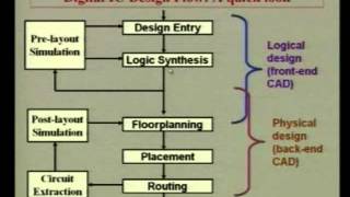
In VLSI design, optimization plays a central role in achieving high efficiency and performance in integrated circuits. This section outlines critical optimization concepts used to enhance circuit designs, highlighting the trade-offs that designers face regarding area, power consumption, performance, and design time. Key optimization strategies include:
- Power Optimization: Techniques such as power gating, clock gating, and dynamic voltage scaling actively contribute to reducing power usage during operation, which is vital in portable and battery-operated devices.
- Area Optimization: Algorithms function to minimize the chip area while ensuring compliance with functional and performance requirements, thus affecting overall costs and layout efficiency.
- Timing Optimization: This ensures that circuits function at designated speeds by minimizing delays across paths, which is crucial for meeting performance benchmarks.
- Signal Integrity: Optimizing interconnects and minimizing crosstalk help preserve signal quality, thus ensuring reliable circuit operation.
These optimization concepts are foundational in the broader context of automation within the VLSI design process, facilitating designers in creating advanced and reliable circuits.
Youtube Videos


Audio Book
Dive deep into the subject with an immersive audiobook experience.
Overview of Optimization in VLSI Design
Chapter 1 of 5
🔒 Unlock Audio Chapter
Sign up and enroll to access the full audio experience
Chapter Content
Optimization in VLSI design involves making trade-offs between various factors like area, power consumption, performance, and design time. These optimizations are achieved through algorithmic approaches and by using specialized CAD tools.
Detailed Explanation
In VLSI design, optimization is all about improving the design of integrated circuits. Designers must balance several different factors: the physical area the circuit occupies on a chip, how much power it consumes, its performance speed, and the time it takes to design it. To optimize, designers utilize algorithms—step-by-step computational procedures—and sophisticated software tools known as CAD (Computer-Aided Design) tools.
Examples & Analogies
Think of a VLSI designer as a chef creating the perfect recipe. The chef must balance flavors, ingredients, cooking time, and presentation to create a dish that satisfies everyone. Similarly, the VLSI designer mixes various design factors to create an efficient circuit.
Power Optimization Techniques
Chapter 2 of 5
🔒 Unlock Audio Chapter
Sign up and enroll to access the full audio experience
Chapter Content
Power Optimization: Techniques such as power gating, clock gating, and dynamic voltage scaling help in reducing power consumption.
Detailed Explanation
Power optimization is essential in VLSI design to ensure that the integrated circuits do not consume excessive energy. Techniques like power gating can turn off parts of the circuit that aren't in use, similar to switching off lights in unoccupied rooms. Clock gating stops the clock signal to certain components when they are idle, preventing unnecessary power usage. Dynamic voltage scaling adjusts the voltage supplied to the circuit based on workload, allowing for power savings during lower performance needs.
Examples & Analogies
Imagine an office building where lights in rooms are turned off when no one is inside. This saves electricity. In the same way, power optimization techniques help circuits use only the energy they need, similar to saving power in a building.
Area Optimization Algorithms
Chapter 3 of 5
🔒 Unlock Audio Chapter
Sign up and enroll to access the full audio experience
Chapter Content
Area Optimization: Algorithms that minimize chip area while ensuring that the design meets the functional and performance requirements.
Detailed Explanation
Area optimization focuses on reducing the physical size of the chip without sacrificing performance or functionality. Algorithms are employed to rearrange circuit components in a way that they occupy less space, ensuring that even as they shrink, they still function correctly and fast. This is important because a smaller chip often leads to lower manufacturing costs.
Examples & Analogies
Consider packing a suitcase for a trip. You want to fit as much as possible into a small space while ensuring that everything you need is included. Area optimization is akin to the strategic packing strategies you use to make the best use of limited luggage space.
Timing Optimization
Chapter 4 of 5
🔒 Unlock Audio Chapter
Sign up and enroll to access the full audio experience
Chapter Content
Timing Optimization: Ensures that the circuit meets the required speed by optimizing the delay of paths in the design.
Detailed Explanation
Timing optimization is essential for ensuring that the circuit operates at the required speed. This involves analyzing the pathways that signals travel within the design and adjusting them to minimize delays. If a signal takes too long to propagate from one section to another, it can slow down the entire circuit, leading to performance issues.
Examples & Analogies
Think of a relay race where a delay in passing the baton can slow down the entire team. Similarly, ensuring that electrical signals move promptly through the circuit is crucial for optimal performance.
Signal Integrity Optimization
Chapter 5 of 5
🔒 Unlock Audio Chapter
Sign up and enroll to access the full audio experience
Chapter Content
Signal Integrity: Optimizing interconnects and minimizing crosstalk between signals to maintain signal quality.
Detailed Explanation
Signal integrity optimization focuses on ensuring that the signals transmitted through the circuit remain clear and strong. This involves optimizing the connections (interconnects) between components and reducing crosstalk, which is the interference caused by signals from adjacent lines. High signal integrity is critical to ensure that the circuit functions as intended without errors.
Examples & Analogies
Imagine a crowded conversation at a party where voices overlap, making it difficult to hear one person clearly. Reducing noise and ensuring each voice is distinct is akin to optimizing signal integrity in circuits, where clarity is essential for precise communication.
Key Concepts
-
Optimization Techniques: Strategies to improve various aspects like power, area, and performance in VLSI designs.
-
Power Gating: A method of turning off certain components of a circuit to save energy when not in use.
-
Clock Gating: Technique to prevent the propagation of clock signals to inactive circuits to minimize power consumption.
-
Dynamic Voltage Scaling: Adjusting the voltage supply to the circuit depending on the operational demand to enhance power efficiency.
-
Timing Optimization: Ensuring designs meet specified timing constraints by minimizing delays.
-
Signal Integrity: Maintaining the quality of signal transmission across circuit components to avoid data errors.
Examples & Applications
Using clock gating, a designer can deactivate the clock signal to a block that is not currently active, reducing power without affecting performance.
Dynamic voltage scaling can be utilized in mobile devices where processing demand varies, providing high performance when needed while conserving battery life during idle periods.
Memory Aids
Interactive tools to help you remember key concepts
Rhymes
In VLSI, we optimize, Power and area, we devise. Timing and signals, all in line, Creating circuits that shine.
Stories
Imagine a busy city. Power optimization is like scheduling traffic lights, ensuring energy is conserved when roads are empty. Area optimization is akin to using space efficiently for buildings without making the city cramped. Timing is like a synchronized show where signals must arrive on cue!
Memory Tools
Remember 'PATS' for Power, Area, Timing, and Signal Integrity. Keep these in mind for effective design!
Acronyms
PATS stands for Power, Area, Timing, and Signal Integrity, key aspects of VLSI optimization.
Flash Cards
Glossary
- Power Optimization
Techniques aimed at reducing power consumption in VLSI circuits, such as power gating and dynamic voltage scaling.
- Area Optimization
Strategies implemented to minimize the area occupied by the circuit design while maintaining performance.
- Timing Optimization
The process of ensuring that signals reach their destination within the required timing constraints to avoid functional errors.
- Signal Integrity
The maintenance of the quality of an electrical signal as it travels through a circuit, minimizing issues like crosstalk.
Reference links
Supplementary resources to enhance your learning experience.