
Introduction to Physical Design in VLSI
Enroll to start learning
You’ve not yet enrolled in this course. Please enroll for free to listen to audio lessons, classroom podcasts and take practice test.
Interactive Audio Lesson
Listen to a student-teacher conversation explaining the topic in a relatable way.
Introduction to Physical Design
🔒 Unlock Audio Lesson
Sign up and enroll to listen to this audio lesson

Today, we'll begin by understanding what physical design in VLSI is. Can anyone tell me why this phase is crucial?

It's where logical designs become real layouts that can be manufactured, right?
Exactly! Physical design is all about taking those logical representations and turning them into tangible layouts. It involves optimizing for performance, area, and power. Remember the acronym P.A.P. for Physical design – Performance, Area, and Power!

What does that mean in practical terms?
Good question! It means we want to make sure the layout is efficient, fits into the chip, and works within the power limits.
Key Processes in Physical Design
🔒 Unlock Audio Lesson
Sign up and enroll to listen to this audio lesson

Now, let’s dive into the major steps of physical design. Can anyone identify the three main processes involved?

Floorplanning, placement, and routing?
That's right! Floorplanning sets the initial layout, placement assigns specific locations to designs, and routing connects these designs together. Can anyone explain why these steps are interconnected?

If the floorplan is not done right, placement and routing will also face problems, like excessive wirelength or timing issues.
Exactly! Each step influences the next. Keep in mind the flow: Floorplanning → Placement → Routing.
Goals of Physical Design
🔒 Unlock Audio Lesson
Sign up and enroll to listen to this audio lesson
What would you say are the goals of physical design?
To ensure that the design fits in the silicon area and meets performance requirements?
Correct! Additionally, we seek to optimize for power consumption. Can anyone think of why power optimization is so crucial?
Because power consumption affects the heat generated, which can lead to failure?
Well said! Power efficiency is vital for modern electronics. Great insights today, everyone!
Introduction & Overview
Read summaries of the section's main ideas at different levels of detail.
Quick Overview
Standard
The physical design stage of VLSI design is fundamental as it converts logical designs into manufacturable layouts. This section details floorplanning, placement, and routing as key processes that optimize the performance and efficiency of the circuit layout within specified constraints.
Detailed
Introduction to Physical Design in VLSI
Physical design represents a pivotal step in the VLSI design flow. This process converts abstract logical representations of a circuit into concrete physical layouts that can be fabricated. It encompasses a variety of essential tasks like floorplanning, placement, routing, and optimization, all aimed at adhering to crucial constraints related to performance, area, and power usage.
The essence of physical design lies in its efficiency in utilizing silicon real estate, while ensuring compliance with functional specifications and manufacturability requirements. In this chapter, we delve deep into the critical algorithms employed throughout the physical design journey, primarily focusing on the three main stages of optimization: floorplanning, placement, and routing.
Youtube Videos
Audio Book
Dive deep into the subject with an immersive audiobook experience.
Overview of Physical Design
Chapter 1 of 4
🔒 Unlock Audio Chapter
Sign up and enroll to access the full audio experience
Chapter Content
Physical design is the final step in the VLSI design flow, where logical representations of the circuit are transformed into a physical layout that can be fabricated.
Detailed Explanation
In the realm of very-large-scale integration (VLSI), physical design refers to the process of translating the abstract, logical schematic diagrams of electronic circuits into a physical arrangement that can be fabricated onto silicon wafers. This transformation is crucial because while designers can create efficient circuitry on paper, the real challenge lies in how to fit this design onto a chip in a way that is manufacturable.
Examples & Analogies
Think of this process like building a city. The logical design is like the city planner's blueprint, showing what each building will be and where it should be located. However, to build the city, you need to physically place each building on the land, ensuring there is space for roads and utilities—much like how engineers layout chips.
Key Tasks in Physical Design
Chapter 2 of 4
🔒 Unlock Audio Chapter
Sign up and enroll to access the full audio experience
Chapter Content
This stage involves critical tasks such as floorplanning, placement, routing, and optimization to meet performance, area, and power constraints.
Detailed Explanation
Several critical tasks fall under the physical design process. These include:
Examples & Analogies
Imagine organizing a large event where you need to consider various elements. You first plan the layout of the venue (floorplanning), then decide where each booth or stage will go (placement), ensuring that pathways between them are clear (routing), and finally, you make adjustments to ensure everything fits within the venue and runs smoothly (optimization).
Goals of Physical Design
Chapter 3 of 4
🔒 Unlock Audio Chapter
Sign up and enroll to access the full audio experience
Chapter Content
The goal of physical design is to efficiently use available silicon real estate while ensuring that the design meets the required functional specifications, performance metrics, and manufacturability requirements.
Detailed Explanation
The physical design phase has several objectives. First, it aims to utilize the available space on the silicon chip efficiently—this is essential since chip areas are expensive to manufacture. Second, the design must adhere to functional requirements, ensuring that the circuit performs its intended functions correctly. Additionally, performance metrics, such as speed and power consumption, must be met, along with manufacturability criteria, making it possible to fabricate the design without defects.
Examples & Analogies
Consider packing for a vacation. You have limited suitcase space (silicon area), and you want to fit all necessary items (functional specifications) while keeping your luggage light (performance metrics). You must also ensure your bag is organized enough to allow quick access during your travels (manufacturability).
Focus of the Chapter
Chapter 4 of 4
🔒 Unlock Audio Chapter
Sign up and enroll to access the full audio experience
Chapter Content
This chapter provides an in-depth study of the key algorithms used in the physical design process, focusing on floorplanning, placement, and routing, which are the three main stages of physical design optimization.
Detailed Explanation
The chapter will delve into the specific algorithms that facilitate the physical design process. These algorithms are essential for successfully completing the various stages of design optimization—floorplanning (deciding the layout of blocks), placement (assigning specific locations to each block), and routing (connecting the blocks with wires). Each of these stages has its own set of challenges and solutions, which will be explored in detail throughout the chapter.
Examples & Analogies
It's akin to constructing a building. First, you need to design the layout of different floors (floorplanning), then decide where to put each room within that layout (placement), and finally, establish how to route utilities like electrical wiring through the building (routing). Each step is crucial for the overall success of the project.
Key Concepts
-
Physical Design: Involves transforming logical representations to functional layouts for manufacturing.
-
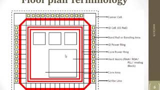
Floorplanning: Determines the placement of functional blocks to enhance performance.
-
Placement: Assigns positions to standardized cells within the predefined layout.
-
Routing: Connects the cells with pathways ensuring compliance with design rules.
Examples & Applications
Example of floorplanning: Arranging storage units in a warehouse for optimal access.
Example of placement: Allocating office desks in an open space to reduce walking time.
Memory Aids
Interactive tools to help you remember key concepts
Rhymes
In VLSI, we design with care; Floorplan, place, route, everywhere!
Stories
Imagine a city planner organizing a city. First, they layout areas (floorplanning), then assign where people live (placement), and finally connect roads (routing).
Memory Tools
Remember 'P.A.P' - Performance, Area, Power for physical design!
Acronyms
F.P.R. - Floorplanning, Placement, Routing
the trio to remember in VLSI design!
Flash Cards
Glossary
- Physical Design
The process of converting logical circuit representation into a physical layout for manufacturing.
- Floorplanning
The process of determining the relative positions of various blocks/modules on a chip.
- Placement
The assignment of positions for standard cells or blocks on a chip after floorplanning.
- Routing
The method of connecting the placed cells or blocks with metal layers to create the final circuit.
- Optimization
Adjusting a design to maximize performance and efficiency while meeting set constraints.
Reference links
Supplementary resources to enhance your learning experience.