
Physical Design and Optimization: Algorithms for Floorplanning, Placement, and Routing
Enroll to start learning
You’ve not yet enrolled in this course. Please enroll for free to listen to audio lessons, classroom podcasts and take practice test.
Interactive Audio Lesson
Listen to a student-teacher conversation explaining the topic in a relatable way.
Introduction to Physical Design in VLSI
🔒 Unlock Audio Lesson
Sign up and enroll to listen to this audio lesson

Today, we are diving into the world of Physical Design in VLSI. This stage is crucial as it transforms logic circuits into physical layouts that can be fabricated. Why do you think this transformation is important?

Because it makes sure that the design can actually be built in real-world applications.
Correct! Physical Design ensures our circuits function as intended, while also meeting performance and area constraints. Can anyone list some key tasks involved in this stage?

There’s floorplanning, placement, and routing, right?
Exactly! These tasks help optimize available silicon space and ensure efficiency. Remember, we want to efficiently utilize silicon real estate while maintaining manufacturability.
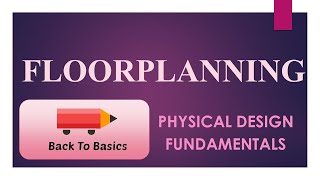
Floorplanning in VLSI Design
🔒 Unlock Audio Lesson
Sign up and enroll to listen to this audio lesson

Now, let’s talk about floorplanning. It focuses on positioning various blocks to optimize area usage. What are some objectives of floorplanning?

Minimizing wirelength and ensuring timing optimization.
Great! Minimizing wirelength is crucial because it impacts power consumption and performance. We have two main types of algorithms for floorplanning: analytical and partitioning. Can anyone explain the difference?

Analytical algorithms use math models while partitioning algorithms break up the layout into smaller parts.
Exactly! Remember our key algorithm, the Kernighan-Lin, which helps with partitioning by minimizing interconnections. This is a great example of the practical application of theories.
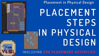
Placement in VLSI Design
🔒 Unlock Audio Lesson
Sign up and enroll to listen to this audio lesson
Next is placement, which assigns positions to blocks after floorplanning. Students, can you tell me the main goals of placement?
We want to minimize wirelength and also manage timing!
True! Plus, we aim for density control to avoid manufacturing issues. What are some placement algorithms we might use?
Simulated annealing is one, right?
Absolutely! Simulated annealing helps avoid getting stuck in local minima. Also, there are greedy algorithms, and quadratic programming for optimization. Can anyone think of a practical example of how we would apply these?
We could use simulated annealing to iteratively find the best block placements based on wirelength.
Exactly! By positioning related cells closer, we reduce wirelength, which is critical for circuit performance.
Routing in VLSI Design
🔒 Unlock Audio Lesson
Sign up and enroll to listen to this audio lesson
Moving on to routing, which connects our designs. What's the primary goal of routing?
To connect cells while keeping the routing length minimized.
Correct! We have global and detailed routing—can anyone explain the difference?
Global routing finds general routes, while detailed routing finalizes precise paths.
Exactly! Algorithms like Maze routing and A* are crucial in this process. Remember that a well-optimized routing is essential for minimizing delays in performance.
And optimizing the layer assignment is also important to avoid congestion!
Right! Congestion can really impact the efficiency of our circuit.
Optimization Techniques
🔒 Unlock Audio Lesson
Sign up and enroll to listen to this audio lesson
Finally, let’s discuss optimization techniques in routing. Why do we need to optimize routing?
To ensure our design is efficient and meets performance standards.
Exactly! Congestion avoidance, layer assignment, and timing-driven routing are key techniques. By properly assigning layers and ensuring critical signals are prioritized, we enhance performance and manufacturability.
So it's about balancing multiple factors to find the best configuration?
Yes! That balance is vital in modern VLSI designs. Great job today, everyone. Remember, these concepts will be crucial as we delve deeper into VLSI complexities.
Introduction & Overview
Read summaries of the section's main ideas at different levels of detail.
Quick Overview
Standard
This chapter delves into the crucial algorithms involved in the physical design process of VLSI, including the key stages of floorplanning, placement, and routing. It highlights the goals of optimizing area, minimizing wirelength, and ensuring manufacturability, while providing insights into various analytical and partitioning algorithms used in each stage.
Detailed
Detailed Summary
Chapter 5 explores the essential role of physical design in VLSI (Very Large Scale Integration) circuit development. Physical design is the final phase where logical representations of circuits are translated into physical layouts suitable for fabrication. This transformation includes several critical tasks like floorplanning, placement, and routing, which aim to meet vital performance, area, and power constraints. The optimization of silicon real estate is paramount to ensure that not only do the designs meet functional specifications but also that they can be manufactured effectively.
5.1 Introduction to Physical Design in VLSI
Physical design connects logical design with real-world fabrication, emphasizing techniques to optimize layout for performance, size, and power consumption.
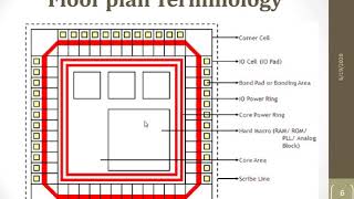
5.2 Floorplanning in VLSI Design
Floorplanning arranges the relative positions of functional blocks to optimize area usage while minimizing delays. Important objectives include block placement, wirelength minimization, and timing optimization. The algorithms can be divided into:
- Analytical Algorithms: Use mathematical models for optimization, such as simulated annealing and force-directed methods.
- Partitioning Algorithms: Break the design into manageable partitions for efficient placement, exemplified by the Kernighan-Lin algorithm.
5.3 Placement in VLSI Design
Placement follows floorplanning and focuses on positioning standard cells on the chip. Key optimization goals include wirelength minimization, timing optimization, and density control. Placement algorithms are categorized into:
- Global Placement: Coarse placement to minimize wirelength.
- Detailed Placement: Fine adjustment for manufacturing specifics.
5.4 Routing in VLSI Design
Routing interconnects cells or blocks, ensuring connections are made while minimizing routing length and avoiding timing issues. Routing processes include:
- Global Routing: Finding general routes without layout details.
- Detailed Routing: Finalizing exact wire paths and avoiding overlaps.
5.5 Optimization Techniques in Routing
Routing optimization is critical for efficiency and manufacturability. Key techniques include congestion avoidance, layer assignment, and timing-driven routing.
5.6 Conclusion
The chapter concludes that mastering these algorithms is imperative to evolving VLSI design, especially as circuit complexity increases, necessitating sophisticated optimization methods.
Youtube Videos
Audio Book
Dive deep into the subject with an immersive audiobook experience.
Introduction to Physical Design in VLSI
Chapter 1 of 5
🔒 Unlock Audio Chapter
Sign up and enroll to access the full audio experience
Chapter Content
Physical design is the final step in the VLSI design flow, where logical representations of the circuit are transformed into a physical layout that can be fabricated. This stage involves critical tasks such as floorplanning, placement, routing, and optimization to meet performance, area, and power constraints. The goal of physical design is to efficiently use available silicon real estate while ensuring that the design meets the required functional specifications, performance metrics, and manufacturability requirements. This chapter provides an in-depth study of the key algorithms used in the physical design process, focusing on floorplanning, placement, and routing, which are the three main stages of physical design optimization.
Detailed Explanation
In VLSI (Very Large Scale Integration) design, the physical design is an essential last step that converts the theoretical aspects of circuit design into something tangible—essentially, a blueprint for building the circuit on silicon. This conversion includes multiple tasks: floorplanning (arranging blocks of the circuit), placement (determining exact coordinates of these blocks), and routing (connecting these blocks with wires while obeying design rules). The goal is to create a layout that's compact and functions well in terms of speed and power usage, thereby optimizing the use of the limited space available on the chip.
Examples & Analogies
Think of physical design like organizing a large construction site. Just as a construction manager must strategically place materials and equipment to avoid waste and ensure smooth operation, an engineer designing a chip must carefully arrange circuitry to minimize space and optimize performance. If bricks (blocks of circuitry) are scattered randomly, it leads to increased costs (longer wiring and more power consumption) and delays in construction (slower processing power of the chip).
Floorplanning in VLSI Design
Chapter 2 of 5
🔒 Unlock Audio Chapter
Sign up and enroll to access the full audio experience
Chapter Content
Floorplanning is the process of determining the relative positions of the various blocks or modules of a chip to optimize area usage and minimize interconnect delays. The primary goal of floorplanning is to create an initial layout that satisfies the design’s area constraints and optimizes the placement of blocks to minimize wirelength and power consumption. Key objectives in floorplanning include: Block Placement: Determining the relative positions of functional blocks to minimize area and wirelength.
Wirelength Minimization: Minimizing the total length of the interconnects between blocks.
Timing Optimization: Ensuring that critical paths are not too long to avoid timing issues. Floorplanning algorithms can be broadly classified into two categories: Analytical Algorithms: These algorithms use mathematical models to optimize the floorplan. They are often based on concepts from operations research and use techniques like simulated annealing or force-directed methods.
Partitioning Algorithms: These algorithms divide the chip into smaller partitions and then place these partitions in the most efficient manner. One of the most well-known partitioning algorithms is Kernighan-Lin.
Detailed Explanation
Floorplanning in VLSI design is crucial because it sets the stage for the chip's layout. The process involves placing various blocks in such a way that uses area efficiently, reduces the distance interconnections need to travel (which minimizes delays), and meets specific constraints about area. There are two main types of algorithms used: analytical and partitioning. Analytical algorithms often utilize complex mathematical approaches (like simulated annealing) to find a nearly optimal arrangement, while partitionary algorithms break the design into smaller pieces to manage it better. Both approaches have their advantages, focusing on minimizing area and interconnect length.
Examples & Analogies
Imagine you are designing a small park. You need to decide where to place the benches, flower beds, and pathways. If everything is spaced too far apart, visitors must walk long distances, which can be tiring (similar to interconnect delays). By placing items closer together, the layout becomes more efficient, allowing visitors to enjoy the park without excessive walking. In VLSI design, floorplanning follows a similar approach, organizing circuit blocks for optimal performance and reduced length of connection paths.
Floorplanning Algorithms
Chapter 3 of 5
🔒 Unlock Audio Chapter
Sign up and enroll to access the full audio experience
Chapter Content
Floorplanning algorithms can be broadly classified into two categories: Analytical Algorithms: These algorithms use mathematical models to optimize the floorplan. They are often based on concepts from operations research and use techniques like simulated annealing or force-directed methods.
Partitioning Algorithms: These algorithms divide the chip into smaller partitions and then place these partitions in the most efficient manner. One of the most well-known partitioning algorithms is Kernighan-Lin.
Detailed Explanation
Two main types of algorithms help with floorplanning. Analytical algorithms utilize mathematical models and methods from operations research to find an optimal physical layout by analyzing patterns and configuration options. For instance, simulated annealing is a popular method that mimics physical processes to explore the layout space extensively. On the other hand, partitioning algorithms break down the design into smaller, more manageable sections before working on placing them effectively. This method helps ensure that there aren't any oversights in layout optimizations since each partition can be focused on more closely.
Examples & Analogies
Think of floorplanning algorithms like different techniques for arranging furniture in a room. An analytical algorithm is akin to creating a detailed plan with drawings and measurements to ensure every piece fits perfectly. Contrastingly, a partitioning approach could be like sectioning off the room into areas (like a reading nook and a gaming corner), arranging furniture in each space, and then re-evaluating how to arrange the transitions between the sections. This dual approach can lead to a more functional and visually appealing result.
Placement in VLSI Design
Chapter 4 of 5
🔒 Unlock Audio Chapter
Sign up and enroll to access the full audio experience
Chapter Content
Placement is the process of assigning the positions of standard cells or blocks on the chip after floorplanning. The primary objective is to minimize the total wirelength and meet timing constraints, while also ensuring the design fits within the chip's available area.
Detailed Explanation
Once the floorplan is laid out, placement comes next. This stage involves positioning the actual components—like cells and blocks of the chip—based on the floorplan created earlier. The main goals here are to place the components close to one another to reduce wiring length (which can slow down the circuit) and to make sure that the timing of signals through the circuit meets required constraints. An effective placement can enhance the performance and efficiency of the resulting circuit.
Examples & Analogies
Think of placement like arranging ingredients in a kitchen. When you are cooking, it's helpful to have common ingredients close to each other to minimize the time spent moving around. If all spices are clustered together, compared to having them spread out around the kitchen, you can quickly reach and grab what you need. In VLSI design, optimal placement means keeping related components close to reduce the time it takes to send signals throughout the chip.
Routing in VLSI Design
Chapter 5 of 5
🔒 Unlock Audio Chapter
Sign up and enroll to access the full audio experience
Chapter Content
Routing is the process of connecting the cells or blocks placed in the previous steps with metal layers to form the complete circuit. The goal is to ensure that all connections are made while minimizing the total routing length, reducing power consumption, and avoiding timing violations.
Detailed Explanation
Routing is the final step after floorplanning and placement, where actual connections are established between the various components on the chip using metal wires. The focus here is on ensuring that every cell and block is properly connected while keeping the routing paths as short as possible. Shorter paths lead to lower power consumption and improve the overall performance of the circuit. Many factors come into play, such as avoiding overlaps between wires and managing the timing of signal transitions.
Examples & Analogies
Routing can be likened to setting up electrical wiring in a new house. An electrician must run wires between outlets, switches, and fixtures, ensuring that everything is connected efficiently. They need to minimize the amount of wire used while making sure not to run into problems like overloading circuits or having wires cross and create hazards. Similarly, in VLSI design, effective routing ensures that all components are connected properly without creating issues.
Key Concepts
-
Physical Design: The final stage in VLSI design that translates logical representations into physical layouts.
-
Floorplanning: Involves optimizing the arrangement of functional blocks on a chip.
-
Placement: The positioning of standard cells post-floorplanning to reduce wirelength and meet design constraints.
-
Routing: The connection of components using metal layers to form a complete circuit layout.
Examples & Applications
Using simulated annealing to iteratively optimize block placements while minimizing overall wirelength.
Applying the Kernighan-Lin algorithm for partitioning in a layout design to reduce interconnections.
Memory Aids
Interactive tools to help you remember key concepts
Rhymes
Floorplanning is where we place, to keep our chips running the race.
Stories
A team of engineers designed a new circuit, but it could not connect properly. They discovered that by thoughtful floorplanning, ensuring blocks were close together like friends at a party, they reduced delays and made the circuit faster.
Memory Tools
FPR: Floorplanning, Placement, Routing—these are the key alignments for laying out VLSI circuits.
Acronyms
PRF
Placement Reduces Fatigue—here
‘fatigue’ refers to reduced wirelength and optimized performance.
Flash Cards
Glossary
- VLSI
Very Large Scale Integration, a process of creating integrated circuits by combining thousands of transistors into a single chip.
- Floorplanning
The process of determining the relative positions of blocks in a chip layout to optimize area usage and minimize interconnect delays.
- Placement
The assignment of positions for standard cells or blocks on a chip after floorplanning, focusing on minimizing wirelength and timing.
- Routing
The process of connecting different components of a circuit via metal layers while minimizing routing length and avoiding timing violations.
- Simulated Annealing
A heuristic optimization method inspired by the annealing process in metallurgy for solving floorplanning and placement problems.
- KernighanLin Algorithm
An algorithm used for partitioning a layout to minimize the number of interconnections between different partitions.
- Maze Routing
A classical algorithm for routing that finds the shortest path while avoiding obstacles within a defined area.
Reference links
Supplementary resources to enhance your learning experience.