
Device Physics of Compound Semiconductors
Interactive Audio Lesson
Listen to a student-teacher conversation explaining the topic in a relatable way.
Introduction to Compound Semiconductors
🔒 Unlock Audio Lesson
Sign up and enroll to listen to this audio lesson

Today, we’ll dive into the physics of compound semiconductors, particularly what differentiates them from silicon. Who can tell me what a compound semiconductor is?

A semiconductor made from two or more elements!
Exactly! For example, gallium arsenide (GaAs) is a compound semiconductor. Why do you think this might be important?

They might have different electrical properties than silicon?
Correct! They exhibit unique characteristics such as direct bandgaps. Remember, direct means they can efficiently recombine electrons and holes, emitting light. Let's use the mnemonic 'LED' - Light Emitting Diode to link this idea. What's the significance of the direct bandgap in devices like LEDs?

It lets them produce light efficiently!
Absolutely! Now, let's summarize: compound semiconductors differ in structure from silicon and have unique properties that allow for advanced applications in optoelectronics.
High Electron Mobility and Carrier Transport
🔒 Unlock Audio Lesson
Sign up and enroll to listen to this audio lesson

Next, let’s talk about high electron mobility. Can anyone explain why this is beneficial for semiconductors?
High mobility means electrons can move faster!
Exactly! In GaAs, the mobility can reach around 8500 cm²/V·s compared to about 1500 for silicon. What does this imply for device speed?
Devices can switch on and off faster!
Right again! This feature makes compound semiconductors ideal for applications like HEMTs used in high-frequency communications. Let’s use the acronym 'SPEED' - which stands for Switching Performance, Efficiency, Electronic Devices.

Got it! SPEED highlights the importance of mobility!
Great summary! Remember, high mobility is crucial for rapid carrier transport in electronic applications.
Polarization Effects
🔒 Unlock Audio Lesson
Sign up and enroll to listen to this audio lesson
Now we shift our focus to polarization effects in materials like GaN. What does polarization in semiconductors mean?
It has to do with the arrangement of atoms, right?
Exactly! In Wurtzite structures, there's spontaneous and piezoelectric polarization. Why do you think this can be beneficial?
It creates charge at junctions, which can help with current flow!
Spot on! This charge creates a 2D electron gas, essential for HEMTs. Let's use the memory aid 'TWO' - 'Charge at Two-dimensional interface for Oxygen Hole-to-electron transport.' How does this feature impact device performance?
Improves speed and reduces noise?
Absolutely! This is a significant advantage of compound semiconductors in electronics, leading to low noise and high-speed applications.
Comparison of Silicon and Compound Semiconductors
🔒 Unlock Audio Lesson
Sign up and enroll to listen to this audio lesson
Lastly, let's compare silicon devices with compound semiconductor devices. What do you think are the main differences?
Silicon has an indirect bandgap, right? So, it wouldn’t be great for light emission.
Exactly, silicon’s indirect bandgap makes it poor for optoelectronic applications. On the other hand, compound semiconductors are primarily direct. Remember the rule ‘LAMP’ - Light emission, Applications, Mobility, Performance. What does this tell us about overall applications?
That they excel in communications and high-frequency devices?
Absolutely right! They are highly effective in specialized applications. Let’s summarize: compound semiconductors outperform silicon in several critical aspects including speed, light emission, and efficiency.
Introduction & Overview
Read summaries of the section's main ideas at different levels of detail.
Quick Overview
Standard
The discussion highlights the critical physical principles affecting compound semiconductor devices, including their direct bandgap, high electron mobility, and polarization effects. These features lead to the superior performance of devices such as HEMTs, LEDs, and laser diodes in high-speed and optoelectronic applications.
Detailed
Device Physics of Compound Semiconductors
This section explains the essential features of compound semiconductors that lead to their superior performance over traditional elemental semiconductors like silicon. Compound semiconductors possess unique material properties, including direct vs. indirect bandgap distinctions, high carrier mobility, and varying polarization effects. The chapter elaborates on the direct bandgap characteristic that allows for efficient electron-hole recombination, making these materials suitable for optoelectronic applications like LEDs and laser diodes.
The discussion includes the importance of high electron mobility and high saturation velocity, which facilitate faster switching and operation in devices such as High Electron Mobility Transistors (HEMTs). Additionally, polarization phenomena in compounds like GaN and AlGaN are crucial for developing two-dimensional electron gas systems that enhance performance in high-frequency applications. The section concludes with a comparison to silicon, emphasizing the advantages in speed, light emission, and thermal conductivity for compound semiconductors.
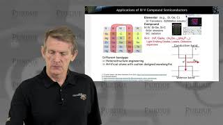
Youtube Videos


Audio Book
Dive deep into the subject with an immersive audiobook experience.
Introduction to Compound Semiconductors
Chapter 1 of 3
🔒 Unlock Audio Chapter
Sign up and enroll to access the full audio experience
Chapter Content
Compound semiconductors, due to their unique material and structural properties, exhibit device physics characteristics that are fundamentally different—and in many ways superior—to elemental semiconductors like silicon. This chapter delves into the physical principles governing the operation of compound semiconductor-based devices, such as high electron mobility transistors (HEMTs), light-emitting diodes (LEDs), and laser diodes. Understanding these principles is critical for designing efficient high-speed, high-frequency, and optoelectronic devices.
Detailed Explanation
Compound semiconductors are materials made from combinations of two or more elements, unlike elemental semiconductors that consist of a single element, such as silicon. This section explains that compound semiconductors have distinct physical characteristics that allow them to perform better in certain applications compared to silicon. It sets the stage for further examination of how these properties facilitate the operation of devices like HEMTs, LEDs, and laser diodes, all of which play crucial roles in high-speed electronic and optoelectronic applications.
Examples & Analogies
Imagine compound semiconductors as a specialized team of athletes, each with specific skills that allow them to excel in different sports. Just as these athletes outperform generalists in their respective fields, compound semiconductors use their unique properties to stand out in advanced application areas like high-speed communication and efficient light emission.
Key Concepts in Compound Semiconductor Device Physics
Chapter 2 of 3
🔒 Unlock Audio Chapter
Sign up and enroll to access the full audio experience
Chapter Content
Direct vs. Indirect Bandgap
- Direct Bandgap: Enables efficient electron-hole recombination with photon emission.
- Crucial for LEDs, laser diodes, and photodetectors.
- Indirect Bandgap (e.g., Silicon): Inefficient for radiative recombination → unsuitable for optoelectronics.
Carrier Mobility and Saturation Velocity
- High Electron Mobility: Allows faster switching and higher-frequency operation.
- Example: GaAs has ~8500 cm²/V·s mobility vs. ~1500 for silicon.
- High Saturation Velocity: Enables rapid carrier transport under strong electric fields.
Polarization Effects (Spontaneous + Piezoelectric)
- Seen in Wurtzite structures like GaN and AlGaN.
- Polarization charge at heterojunctions creates 2D Electron Gas (2DEG):
- Basis of High Electron Mobility Transistors (HEMTs)
- No doping required → low noise, high speed.
Detailed Explanation
This chunk covers several fundamental principles that define the operations of compound semiconductor devices. It begins with the distinction between direct and indirect bandgaps, where direct bandgaps allow for efficient light emission—an essential feature for devices like LEDs and laser diodes. The next part focuses on carrier mobility, highlighting that materials like Gallium Arsenide (GaAs) have significantly higher carrier mobility compared to silicon, making them ideal for fast switching applications. Finally, it discusses polarization effects, particularly in Wurtzite structures, which can create beneficial properties in devices without needing additional doping, enhancing performance further.
Examples & Analogies
Think of direct bandgap materials like a clear glass that lets light through effortlessly, while indirect bandgap materials are like frosted glass that scatters light. In essence, if you're aiming to design something that needs to emit light efficiently, like a lantern, you'd choose clear glass (direct bandgap). In terms of carrier mobility, consider a racetrack: GaAs acts like a high-speed car on a straight track, while silicon is more like a compact car in a city with traffic lights—it takes longer to reach peak speeds because of various barriers.
Important Device Structures in Compound Semiconductors
Chapter 3 of 3
🔒 Unlock Audio Chapter
Sign up and enroll to access the full audio experience
Chapter Content
Light Emitting Diodes (LEDs)
- Material: GaN (blue/white), InGaN, AlGaAs (red/infrared)
- Working Principle:
- Forward bias → electrons and holes recombine in the active layer → photon emission
- Key Benefit: High quantum efficiency due to direct bandgap
Laser Diodes
- Material: GaAs, InP, InGaAsP
- Structure: P-N junction with feedback cavity
- Operation:
- Stimulated emission when injection current exceeds threshold
- Applications: Optical communication, barcode scanners, medical instruments
High Electron Mobility Transistors (HEMTs)
- Material: AlGaN/GaN, AlGaAs/GaAs
- Structure: Heterojunction with 2DEG channel
- Advantages:
- Extremely high-speed switching
- High-power and high-frequency operation
- Applications: Radar, 5G base stations, satellite communications
Photodetectors and Solar Cells
- Photodetectors: InGaAs (infrared), GaAs (visible to NIR)
- Solar Cells: GaAs, CdTe, InGaP/InGaAs multi-junctions
- Benefits:
- Tunable bandgaps for specific wavelengths
- High efficiency even in thin-film form.
Detailed Explanation
In this chunk, we explore various important devices that utilize compound semiconductors. It covers Light Emitting Diodes (LEDs), which utilize materials like Gallium Nitride (GaN) to emit light efficiently due to their direct bandgap. Laser diodes, which also use compound semiconductors, operate on a principle of stimulated emission and have a feedback mechanism to enhance light production for communication and sensing technologies. High Electron Mobility Transistors (HEMTs) use carefully structured materials to enable very high-speed operations and are crucial in advanced telecommunications. Finally, photodetectors and solar cells employing these semiconductors highlight their ability to capture specific wavelengths of light effectively.
Examples & Analogies
Consider these devices as different types of kitchen appliances. LEDs are like energy-efficient lights in your kitchen, providing bright illumination with minimal waste. Laser diodes are akin to a microwave oven that precisely cooks food using energy waves—they're used in tech for precision tasks. HEMTs are the high-performance blenders that can whip up smoothies in seconds, while photodetectors and solar cells are like your kitchen gardens that can harness and utilize sunshine to grow fresh vegetables, making them perform excellently under the right conditions.
Key Concepts
-
Direct Bandgap: Facilitates efficient light emission in devices like LEDs and laser diodes.
-
High Electron Mobility: Enables quick charge transport, resulting in high-speed device operation.
-
Polarization Effects: Enhance carrier concentration at heterojunctions, improving device efficiency.
-
HEMT: A critical device benefiting from compound semiconductor properties for high-frequency applications.
Examples & Applications
GaAs is used in LEDs due to its direct bandgap, enabling bright and efficient light emission.
HEMTs are employed in 5G technology because of their high-speed switching capabilities.
GaN lasers are used in Blu-ray players and optical communications for their efficient light production.
Memory Aids
Interactive tools to help you remember key concepts
Rhymes
For a compound semiconductor, just remember, the light shines bright, it's the direct delight!
Stories
Imagine a world where all semiconductors are compound. They dance and emit light like fireworks. Every time an electron jumps, a photon pops out, lighting the streets—these are the LEDs.
Memory Tools
For remembering electron mobility, think of the phrase ‘Fast Electrons Move‘ - F.E.M.
Acronyms
TWO for the role of polarization
'Charge at Two-dimensional interfaces for Oxygen Hole-to-electron transport.'
Flash Cards
Glossary
- Compound Semiconductor
A semiconductor made from two or more elements with superior properties compared to elemental semiconductors.
- Direct Bandgap
A type of bandgap that allows for efficient electron-hole recombination leading to photon emission.
- High Electron Mobility
The ability of charge carriers to move quickly through a semiconductor material.
- Polarization Effects
Phenomena arising from the arrangement of charge in materials that can enhance carrier concentration at junctions.
- High Electron Mobility Transistor (HEMT)
A transistor that uses a two-dimensional electron gas to achieve high-speed switching and low noise performance.
Reference links
Supplementary resources to enhance your learning experience.