
Introduction
Interactive Audio Lesson
Listen to a student-teacher conversation explaining the topic in a relatable way.
Unique properties of compound semiconductors
🔒 Unlock Audio Lesson
Sign up and enroll to listen to this audio lesson

Today we will explore the unique properties of compound semiconductors. What do you think sets them apart from silicon?

Maybe it's the materials they are made from?
Exactly! Compound semiconductors consist of two or more elements. This allows them to have properties like a direct bandgap, which is crucial for efficient light emission. Can anyone give an example of a device that uses this property?

LEDs use direct bandgap materials! Like gallium nitride.
Great! Now, why do you think direct bandgap materials are essential for LEDs?

Because they allow for efficient electron-hole recombination.
Correct! Recap: Compound semiconductors provide unique properties such as direct bandgaps that benefit devices like LEDs.
Carrier mobility and polarization effects
🔒 Unlock Audio Lesson
Sign up and enroll to listen to this audio lesson

Let's discuss carrier mobility. Why is it important in semiconductors?

Higher carrier mobility means faster switching, right?
Absolutely! For example, gallium arsenide has a mobility of about 8500 cm²/V·s compared to silicon's 1500 cm²/V·s. This makes compound semiconductors ideal for high-frequency applications. Now, what are polarization effects?
Polarization effects occur in some structures, like GaN, and can influence the formation of two-dimensional electron gases.
Exactly! This characteristic is crucial for devices like HEMTs, which leverage these effects to achieve low noise and high speeds. Quick recap: High carrier mobility enhances speed, and polarization effects contribute to unique device functionalities.
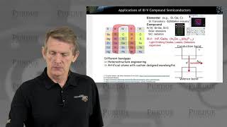
Applications of compound semiconductors
🔒 Unlock Audio Lesson
Sign up and enroll to listen to this audio lesson
Now that we understand the properties, what applications can we identify for compound semiconductors?
Definitely in LEDs and laser diodes!
And in HEMTs for high-speed radio frequency applications!
Exactly! Also consider photodetectors and solar cells as prominent applications where the unique characteristics of compound semiconductors come into play. Recap: The key applications include LEDs, laser diodes, HEMTs, and more.
Introduction & Overview
Read summaries of the section's main ideas at different levels of detail.
Quick Overview
Standard
This section introduces the fundamental principles and characteristics of compound semiconductors, highlighting their advantages over elemental semiconductors like silicon. Focus is placed on the importance of understanding these principles for the design of high-speed and optoelectronic devices.
Detailed
Introduction to Compound Semiconductors
Compound semiconductors possess unique material and structural properties that lead to device physics characteristics fundamentally different from elemental semiconductors like silicon. Key aspects such as direct band gaps, high carrier mobility, and polarization effects enable compound semiconductors to outperform silicon in specific applications. This section lays the foundation for a deeper understanding of the principles governing the operation of various devices, including high electron mobility transistors (HEMTs), light-emitting diodes (LEDs), and laser diodes. Knowledge of these principles is critical for designing efficient, high-speed, high-frequency, and optoelectronic devices.
Youtube Videos


Audio Book
Dive deep into the subject with an immersive audiobook experience.
Overview of Compound Semiconductors
Chapter 1 of 3
🔒 Unlock Audio Chapter
Sign up and enroll to access the full audio experience
Chapter Content
Compound semiconductors, due to their unique material and structural properties, exhibit device physics characteristics that are fundamentally different—and in many ways superior—to elemental semiconductors like silicon.
Detailed Explanation
This chunk introduces compound semiconductors, highlighting that they possess distinct material and structural properties compared to elemental semiconductors, such as silicon. These differences lead to unique device physics characteristics which can often result in superior performance in various applications. Essentially, compound semiconductors are not just variations of silicon but are fundamentally different in their nature and operation.
Examples & Analogies
Think of compound semiconductors like a Swiss Army knife, which has multiple tools and capabilities that allow it to perform many tasks efficiently, compared to a straightforward screwdriver (which represents silicon) that has a single purpose. This illustrates how compound semiconductors can offer more versatile and powerful functionalities in electronic devices.
Importance of Physical Principles
Chapter 2 of 3
🔒 Unlock Audio Chapter
Sign up and enroll to access the full audio experience
Chapter Content
This chapter delves into the physical principles governing the operation of compound semiconductor-based devices, such as high electron mobility transistors (HEMTs), light-emitting diodes (LEDs), and laser diodes.
Detailed Explanation
In this part, the text emphasizes the focus of the chapter on the physical principles that govern how various devices made from compound semiconductors operate. This includes understanding the theoretical and practical aspects that make devices like HEMTs, LEDs, and laser diodes function effectively. By grasping these principles, engineers and scientists can design better and more efficient devices for modern technology.
Examples & Analogies
Consider this like learning the rules of a complex board game. Just like understanding the rules helps you play well, knowing the physical principles helps engineers create advanced electronic devices that work efficiently and effectively.
Applications and Benefits
Chapter 3 of 3
🔒 Unlock Audio Chapter
Sign up and enroll to access the full audio experience
Chapter Content
Understanding these principles is critical for designing efficient high-speed, high-frequency, and optoelectronic devices.
Detailed Explanation
Here, the text underscores the importance of understanding the physical principles, stating that this knowledge is essential to develop efficient devices that operate at high speeds and high frequencies. In the context of today's rapidly advancing technology, being able to design devices that leverage the unique properties of compound semiconductors can lead to innovations in communications, computing, and lighting, among others.
Examples & Analogies
Imagine trying to build a race car without knowing about aerodynamics. Understanding the principles not only helps you to design a fast car but also ensures it runs efficiently on the track, similar to how understanding the principles of compound semiconductors enables the creation of high-performance electronic devices.
Key Concepts
-
Compound Semiconductors: Materials made from multiple elements with unique properties.
-
Direct Bandgap: Allows for efficient electron-hole recombination, key for light-emitting devices.
-
Carrier Mobility: The speed at which charge carriers move in semiconductors, crucial for performance.
-
Polarization Effects: Influences device behavior, particularly in HEMTs.
Examples & Applications
The efficiency of LEDs using Gallium Nitride (GaN) due to its direct bandgap.
The speed advantage of HEMTs over silicon transistors in telecommunications.
Memory Aids
Interactive tools to help you remember key concepts
Rhymes
In GaAs, electrons fly fast, high mobility's a blast!
Stories
A tale of two semiconductors: one slow–Silicon; one fast–GaAs, lighting up the world. Both have their places, but Gallium Arsenide shines brighter in the race!
Memory Tools
Remember 'HEMT' for High-speed Electron Mobility Transistor.
Acronyms
BCD
Bandgap
Carrier mobility
Devices – Key concepts of compound semiconductors.
Flash Cards
Glossary
- Compound Semiconductors
Semiconductors made from two or more elements, exhibiting unique properties distinct from elemental semiconductors.
- Direct Bandgap
A type of bandgap in semiconductors that allows for efficient electron-hole recombination and light emission.
- Carrier Mobility
The ability of charge carriers (electrons and holes) to move through a semiconductor material under the influence of an electric field.
- TwoDimensional Electron Gas (2DEG)
A layer of electrons confined to two dimensions, which forms at the interface of certain semiconductor materials and is utilized in HEMTs.
Reference links
Supplementary resources to enhance your learning experience.