
Introduction
Interactive Audio Lesson
Listen to a student-teacher conversation explaining the topic in a relatable way.
What is a PN Junction?
🔒 Unlock Audio Lesson
Sign up and enroll to listen to this audio lesson

Alright class, let’s start by understanding what a PN junction is. A PN junction is formed when p-type and n-type semiconductor materials are joined together. Who can tell me what p-type and n-type mean?

I think p-type means it has more holes than electrons, right?
Exactly! And n-type has more electrons than holes. This difference in charge carriers is crucial for the PN junction's function. Can anyone explain why we need to go beyond just knowing what these types are?

So we can understand how they behave in circuits under different conditions?
Great point! The behavior of the PN junction changes based on how we apply voltage to it, which leads us to explore biasing conditions.
Biasing Conditions of the PN Junction
🔒 Unlock Audio Lesson
Sign up and enroll to listen to this audio lesson

Now, who can explain what happens when we apply forward bias to a PN junction?

The depletion region gets narrower, and carriers are injected, allowing current to flow.
Correct! And what about reverse bias? What happens there?

The depletion region widens, and minimal current flows, acting like an insulator.
Exactly, and this characteristic is key for devices like diodes. Let's remember the terms 'forward bias' and 'reverse bias' since they represent opposite behaviors.
Importance of the PN Junction
🔒 Unlock Audio Lesson
Sign up and enroll to listen to this audio lesson
Finally, can anyone summarize why the PN junction is so important in electronics?
It’s the building block for many devices like diodes and solar cells!
And it helps in controlling the flow of current in circuits!
Exactly! The principles we discussed today will lead us into more complex concepts like energy band diagrams and the I-V characteristics in the next sections.
Introduction & Overview
Read summaries of the section's main ideas at different levels of detail.
Quick Overview
Standard
This section outlines the importance of the PN junction as the core component in semiconductor devices like diodes and BJTs, formed by joining p-type and n-type materials. It highlights how various biasing conditions affect its operation, setting the stage for deeper exploration in subsequent sections.
Detailed
Introduction to PN Junction
A PN junction is a critical constituent of several semiconductor devices, including diodes, BJTs, solar cells, and LEDs. It is created by the combination of p-type and n-type semiconductor materials, which leads to the formation of unique electrical characteristics that define the function of these devices. The operation of a PN junction varies based on the biasing conditions applied, which influences how it reacts in electrical circuits. Understanding the foundational role of the PN junction is essential for grasping the principles of semiconductor technology.
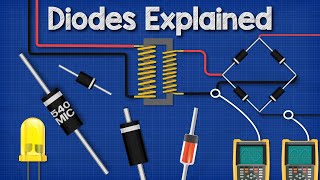
Youtube Videos


Audio Book
Dive deep into the subject with an immersive audiobook experience.
Definition of PN Junction
Chapter 1 of 3
🔒 Unlock Audio Chapter
Sign up and enroll to access the full audio experience
Chapter Content
A PN junction is the fundamental building block of many semiconductor devices such as diodes, BJTs, solar cells, and LEDs.
Detailed Explanation
A PN junction is a type of semiconductor structure that is created by placing p-type (positive) and n-type (negative) semiconductor materials together. This structure is crucial because it forms the basis of many electronic components. The interaction between the p-type and n-type materials allows the PN junction to control the flow of electrical current, making it essential for devices such as diodes and transistors.
Examples & Analogies
Think of a PN junction like a gate at a park. The p-side represents an area where people can enter (the park), while the n-side represents the area where they cannot. The gate controls who can and cannot enter, just like a PN junction controls the flow of current.
Formation of the PN Junction
Chapter 2 of 3
🔒 Unlock Audio Chapter
Sign up and enroll to access the full audio experience
Chapter Content
It is formed by joining p-type and n-type semiconductor materials.
Detailed Explanation
The formation of a PN junction occurs when p-type and n-type materials are brought together. In this process, electrons from the n-side (which is rich in electrons) diffuse into the p-side (which is rich in holes), where they recombine with holes. Similarly, holes from the p-side diffuse into the n-side, where they recombine with electrons. This movement of charge carriers leads to the establishment of a depletion region near the junction where there are no free charge carriers available.
Examples & Analogies
Imagine mixing two different types of liquid, one floating on top of the other. As they mix, some of the top liquid enters the bottom one, and vice versa, creating a clear boundary between the two. This boundary is similar to the depletion region created in a PN junction, where charge carriers have recombined and filled available spaces.
Behavior Under Biasing Conditions
Chapter 3 of 3
🔒 Unlock Audio Chapter
Sign up and enroll to access the full audio experience
Chapter Content
The behavior of the PN junction under different biasing conditions defines its operation in circuits.
Detailed Explanation
The operation of a PN junction depends on how it is biased, meaning whether it is connected to a voltage source in a forward or reverse manner. In forward bias, the p-side is connected to the positive terminal and the n-side to the negative terminal, allowing current to flow. Conversely, in reverse bias, the p-side is connected to the negative terminal, widening the depletion region and preventing current flow. Understanding these conditions is vital for using PN junctions effectively in electronic circuits.
Examples & Analogies
Think of a one-way street that allows cars to go in only one direction when the traffic light is green. In forward bias (green light), cars can move through, while in reverse bias (red light), no cars can pass, and the road is effectively blocked. This is how the PN junction regulates current flow.
Key Concepts
-
PN Junction: The intersection of p-type and n-type materials where unique electronic properties arise.
-
Biasing Conditions: The external voltages applied that influence the behavior of the PN junction.
-
Depletion Region: The area around the junction that is devoid of free carriers, crucial for diode function.
Examples & Applications
PN junctions are used in diodes to allow current to flow in one direction while blocking it in the opposite direction.
They form the basic operational element in a solar cell which converts light energy into electrical energy.
Memory Aids
Interactive tools to help you remember key concepts
Rhymes
In a diode bright and new, P and N can join and do, They charge and flow when biased right, Blocking currents when in reverse fright.
Stories
Imagine two friends, P and N, who meet to create a power duo. When they apply pressure together (forward bias), they can work wonders, allowing flow just like a river. But when they are pushed apart (reverse bias), they block each other, protecting the path.
Memory Tools
Remember: 'P for Plenty of holes, N for No holes.' This helps differentiate p-type and n-type semiconductors.
Acronyms
For the PN junction behavior
for Forward (conducts)
for Reverse (blocks). Keep in mind
Flash Cards
Glossary
- PN Junction
The boundary between p-type and n-type semiconductor materials that creates a diode's fundamental characteristics.
- Ptype Semiconductor
A semiconductor material that has an excess of holes resulting from the addition of acceptor impurities.
- Ntype Semiconductor
A semiconductor material that has an excess of electrons due to the addition of donor impurities.
- Depletion Region
The area around the PN junction where mobile charge carriers have been depleted, forming an insulating barrier.
- Biasing Conditions
The application of an external voltage across the PN junction, which can be forward or reverse.
Reference links
Supplementary resources to enhance your learning experience.