
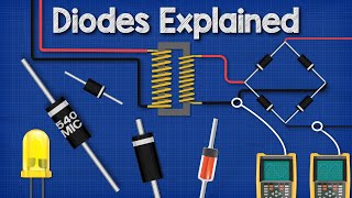
Summary of Key Concepts
Interactive Audio Lesson
Listen to a student-teacher conversation explaining the topic in a relatable way.
Current Directionality
🔒 Unlock Audio Lesson
Sign up and enroll to listen to this audio lesson

Today we’re focusing on the PN junction diode, particularly how it controls current flow. Can anyone tell me what happens when we apply forward bias to a diode?

The current flows through it.
Exactly! In forward bias, the p-side connected to the positive terminal allows electrons from the n-side to flow and recombine with holes. Now, what about reverse bias?

The current doesn’t flow at all.
Right! In reverse bias, it acts like an insulator. Remember the acronym 'FLOWS' for Forward allows current, while 'BLOCKS' for Reverse blocks it. Great job!
Depletion Region and Built-in Potential
🔒 Unlock Audio Lesson
Sign up and enroll to listen to this audio lesson

Let's dive deeper into what happens at the PN junction when it forms. Who can explain the depletion region?

It's an area with no free carriers, just immobile ions.
Exactly! This region is critical because it creates the built-in potential, which is what we rely on in reverse bias. Can anyone explain why this is important?

It prevents electrons from crossing to the p-side.
Perfect! Remember that the built-in potential establishes an internal electric field that is crucial for the diode's operation. Keep these concepts in mind!
Importance in Semiconductor Devices
🔒 Unlock Audio Lesson
Sign up and enroll to listen to this audio lesson
Now that we understand the basics of the PN junction, let’s discuss its applications. Why do you think PN junctions are important in devices like LEDs or solar cells?
Because they control where current flows, which is crucial for the operation of those devices!
Absolutely! They act as a foundation for many electronic components. Can anyone name a few applications?
Rectifiers, Zener diodes, and even LED!
Excellent! The PN junction is indeed foundational. Remember, their behavior under different biasing conditions is key to understanding how these devices function.
Introduction & Overview
Read summaries of the section's main ideas at different levels of detail.
Quick Overview
Standard
This section outlines that the PN junction diode's operation is characterized by its ability to allow current flow in one direction during forward bias while blocking it during reverse bias. Key components such as the depletion region and built-in potential play critical roles in determining this behavior, making the PN junction essential for numerous semiconductor devices.
Detailed
Summary of Key Concepts
The PN junction diode serves as a fundamental component in a wide range of semiconductor devices. Its operation is principal to electronics since it regulates the direction of current flow.
Key Points
- Current Directionality: Under forward bias (where the p-side is connected to a positive terminal), the diode allows current to flow easily. Conversely, in reverse bias (where the p-side connects to a negative terminal), current flow is effectively blocked.
- Depletion Region: This region is vital in determining the diode's functionality. It forms when the p-type and n-type materials are joined, creating immobile ions in a gap devoid of free carriers.
- Built-in Potential: The electric field established in the depletion area creates a potential barrier that is crucial during reverse bias conditions, preventing current flow.
Understanding these aspects of the PN junction diode is critical, as they form the foundation for various linear and non-linear semiconductor devices used in modern electronic applications.
Youtube Videos


Audio Book
Dive deep into the subject with an immersive audiobook experience.
Direction of Current Flow
Chapter 1 of 3
🔒 Unlock Audio Chapter
Sign up and enroll to access the full audio experience
Chapter Content
A PN junction diode allows current flow in one direction under forward bias, and blocks it under reverse bias.
Detailed Explanation
A PN junction diode is designed to conduct current when it is forward biased. This means that when the positive side of the battery is connected to the p-type material and the negative side is connected to the n-type material, electricity can flow. However, if the connections are reversed (reverse bias), the diode will block the current. This property makes diodes useful for controlling the direction of current in electronic circuits.
Examples & Analogies
Think of the diode like a one-way street. Cars (representing current) can travel down the street freely when it flows in the correct direction (forward bias), but if they try to come from the opposite direction (reverse bias), they are stopped by a barrier.
Depletion Region and Built-in Potential
Chapter 2 of 3
🔒 Unlock Audio Chapter
Sign up and enroll to access the full audio experience
Chapter Content
The depletion region, built-in potential, and biasing conditions determine its behavior.
Detailed Explanation
The depletion region is an area near the pn-junction where charge carriers (electrons and holes) have recombined, leaving behind immobile charged ions. This region creates an electric field and a potential barrier that influences how the diode behaves under different biasing conditions. Under forward bias, this barrier is reduced, allowing current to flow easily, while under reverse bias, the barrier is increased, preventing current flow.
Examples & Analogies
You can think of the depletion region like a dam in a river. When the dam (potential barrier) is high (reverse bias), water (current) cannot pass through. But when the dam is lowered (forward bias), the water can flow freely.
Foundation for Semiconductor Devices
Chapter 3 of 3
🔒 Unlock Audio Chapter
Sign up and enroll to access the full audio experience
Chapter Content
The PN junction is the foundation for a wide variety of linear and non-linear semiconductor devices.
Detailed Explanation
The PN junction is crucial in the design and functioning of many semiconductor devices, including diodes, transistors, solar cells, and light-emitting diodes (LEDs). It establishes the basic principles of how these devices operate and interact with electrical signals. Understanding the PN junction allows engineers to innovate and improve existing devices as well as create new ones.
Examples & Analogies
Consider the PN junction to be like the foundation of a building. Just as a sturdy foundation is essential for the stability and safety of a building, the PN junction serves as the essential base for various electronic devices, ensuring they function properly.
Key Concepts
-
Current Directionality: Allows current in forward bias and blocks it in reverse bias.
-
Depletion Region: An area devoid of carriers that forms at the junction.
-
Built-in Potential: Voltage opposing carrier diffusion, crucial in diode functionality.
-
Applications: PN junctions are essential for devices like rectifiers, LEDs, and solar cells.
Examples & Applications
A diode in a smartphone allowing charge to flow to the battery only when charging.
A solar panel utilizing PN junctions to convert sunlight into electrical energy.
Memory Aids
Interactive tools to help you remember key concepts
Rhymes
In forward bias, currents glide, in reverse, they must abide.
Stories
Imagine a gate that only opens when the sun shines, just like how a diode allows current only when it's forward biased.
Memory Tools
'FLOW B' for Forward allows Current, 'BLOCK R' for Reverse blocks it.
Acronyms
FIBER for 'Forward Invites, Backward Excludes, Recessed energy.'
Flash Cards
Glossary
- PN Junction
The boundary between p-type and n-type semiconductor materials, where their properties interact.
- Forward Bias
Connection of the p-side of a diode to a positive terminal, allowing current flow.
- Reverse Bias
Connection of the p-side of a diode to a negative terminal, blocking current flow.
- Depletion Region
The area near the junction where free carriers are depleted, forming immobile ions.
- Builtin Potential
The internal voltage that opposes carrier diffusion across the depletion region.
Reference links
Supplementary resources to enhance your learning experience.