
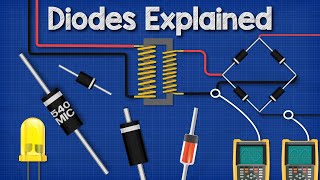
Operation of the PN Junction Diode
Interactive Audio Lesson
Listen to a student-teacher conversation explaining the topic in a relatable way.
Formation of the PN Junction
🔒 Unlock Audio Lesson
Sign up and enroll to listen to this audio lesson

Today, we’re discussing the formation of a PN junction, which is the heart of many electronic devices. Can anyone describe how a PN junction is created?

Is it where the p-type and n-type materials meet?
Exactly! When these materials come together, electrons and holes diffuse across the junction. This interaction leads to the formation of a depletion region that is critical for the diode's operation. Can anyone tell me what a depletion region is?

I think it's the area that lacks free charges, right?
Yes! And it’s filled with immobile ions. This region establishes an internal electric field and a built-in potential. We'll remember this as 'EBD': Electric field, Built-in potential, Depletion region.

What does the built-in potential actually do?
Great question! The built-in potential opposes further diffusion of carriers, which is crucial for how the diode functions.
Biasing the PN Junction
🔒 Unlock Audio Lesson
Sign up and enroll to listen to this audio lesson

Let’s dive into biasing. Can someone explain what happens when we apply forward bias to the PN junction?

I think it makes the current flow more easily.
That's correct! In forward bias, the p-side is connected to the positive terminal, narrowing the depletion region. This allows carriers to flow. What about reverse bias?
Isn’t reverse bias when the p-side is negative? It widens the depletion region, right?
Spot on! In reverse bias, the depletion region widens, and current flow is minimal, acting as an insulator. Remember, ‘WIDEN’ for Reverse Bias: Wider depletion region, Insulator.
What happens to the current in reverse bias?
There’s very little current flow, known as reverse saturation current. Excellent engagement, everyone!
I-V Characteristics of the PN Junction
🔒 Unlock Audio Lesson
Sign up and enroll to listen to this audio lesson
Now, let’s discuss the I-V characteristics of a PN junction diode. Who can share the equation that describes the current in forward bias?
Is it I = I0(e^(qV/kT) - 1)?
Exactly right! This equation shows the exponential relationship between current and voltage. What happens in reverse bias, though?
The current stays constant until breakdown?
Yes! In reverse bias, current saturates at -I0. Understanding these characteristics is essential for designing circuits.
Why do we also need to consider temperature effects on these characteristics?
Excellent point! As temperature increases, reverse saturation current increases, and the threshold voltage decreases. Keep this in mind during project work!
Applications of the PN Junction
🔒 Unlock Audio Lesson
Sign up and enroll to listen to this audio lesson
Finally, let’s talk about the applications of PN junctions. Can anyone name a common application?
Rectifiers for AC to DC conversion!
Correct! Rectifiers are a great application. They convert alternating current to direct current. What else?
How about using them in Zener diodes for voltage regulation?
Exactly! Zener diodes help in voltage regulation. Remember, 'REGULATE' for Regulators, Energy conversion, Generators, Utilization in devices, LEDs, and Applications.
Are they also used in solar cells?
Yes! PN junctions are critical in solar cells for converting light into electricity. Great contributions today!
Introduction & Overview
Read summaries of the section's main ideas at different levels of detail.
Quick Overview
Standard
The PN junction diode is formed by the interaction between p-type and n-type semiconductors, which creates a depletion region. This section covers how biasing affects its operation, summarizes the I-V characteristics, and describes the impact of temperature, capacitance, and special operational modes.
Detailed
Operation of the PN Junction Diode
A PN junction diode is a crucial component in semiconductor devices, formed by combining p-type and n-type materials. When these materials join, electrons from the n-side and holes from the p-side diffuse and recombine, creating a depletion region that is devoid of free charge carriers._ This depletion region establishes an internal electric field and a built-in potential (V_bi), which influences how the diode behaves under various biasing conditions.
Biasing Conditions
- Forward Bias: The p-side is connected to a positive terminal, narrowing the depletion region which allows current to flow as carriers are injected into the junction. The current increases exponentially with voltage based on the relationship I=I0(eqVkT−1).
- Reverse Bias: When the p-side is connected to a negative terminal, the depletion region widens and only a minimal current flows, effectively acting as an insulator.
I-V Characteristics
The diode's behavior can be characterized by its current-voltage relationship, displaying a clear distinction between forwarding and reversing operation. The reverse saturation current (I0) plays a crucial role in this relationship.
Temperature Effects and Applications
Temperature also plays a significant role, with higher temperatures leading to increased leakage currents and decreased threshold voltage. PN junctions are integral in discrete and integrated circuit applications, including rectifiers, voltage regulators, photovoltaic cells, and LED technology. By understanding these characteristics, engineers can utilize PN junctions effectively in circuit design.
Youtube Videos


Audio Book
Dive deep into the subject with an immersive audiobook experience.
Introduction to the PN Junction
Chapter 1 of 3
🔒 Unlock Audio Chapter
Sign up and enroll to access the full audio experience
Chapter Content
A PN junction is the fundamental building block of many semiconductor devices such as diodes, BJTs, solar cells, and LEDs.
- It is formed by joining p-type and n-type semiconductor materials.
- The behavior of the PN junction under different biasing conditions defines its operation in circuits.
Detailed Explanation
The PN junction is essential in electronics as it makes up the basic function of many devices like diodes (which allow current to flow in one direction), BJTs (Bipolar Junction Transistors), solar cells (which convert sunlight into electricity), and LEDs (Light Emitting Diodes).
A PN junction is created when two types of semiconductor materials are combined: p-type, which has a surplus of holes (positive charge carriers), and n-type, which has a surplus of electrons (negative charge carriers).
The way this junction operates will change depending on how it is connected in a circuit, commonly referred to as its 'biasing conditions.' This behavior is crucial in determining how and when current will flow through these devices.
Examples & Analogies
Think of the PN junction like a one-way street: when p-type and n-type materials meet, they create a path that can direct traffic (or electrical current) in a specific direction, but only under certain rules, similar to how a traffic light controls the flow of cars.
Formation of the PN Junction
Chapter 2 of 3
🔒 Unlock Audio Chapter
Sign up and enroll to access the full audio experience
Chapter Content
When p-type and n-type materials are brought together:
- Electrons from the n-side diffuse into the p-side, recombining with holes.
- Holes from the p-side diffuse into the n-side, recombining with electrons.
This leads to the formation of a depletion region near the junction:
- Region devoid of free carriers but filled with immobile ions.
- Establishes an internal electric field and built-in potential (V_bi).
Detailed Explanation
When p-type and n-type semiconductors are joined, there's a diffusion process where the free electrons from the n-side move into the p-side, where they recombine with the holes. Likewise, holes from the p-side can move into the n-side and recombine with electrons. This recombination results in a depletion region, an area where there are no free charge carriers left (no electrons or holes). Instead, this region becomes filled with immobile, charged ions, which leads to an electric field being established across the junction.
This internal electric field creates a barrier that opposes any further movement of charge carriers from one side to the other, establishing what is called the built-in potential (V_bi). This is crucial because it affects how the diode will operate when connected in a circuit.
Examples & Analogies
Imagine mixing oil and water; when they meet, they create a boundary where the two don't mix, similar to how the depletion region acts as a barrier at the junction of p-type and n-type materials. Just as the oil and water create a noticeable layer, the depletion region is the area where charges can’t freely flow.
Energy Band Diagram
Chapter 3 of 3
🔒 Unlock Audio Chapter
Sign up and enroll to access the full audio experience
Chapter Content
At Equilibrium (No External Bias):
- Fermi level is constant across the junction.
- Conduction and valence bands bend due to the internal electric field.
- The built-in potential (V_bi) opposes further diffusion of carriers.
Detailed Explanation
In a PN junction at equilibrium (meaning there is no external voltage applied), the Fermi level, which indicates the energy levels of electrons, becomes constant across the junction. However, the conduction band (where electrons can move freely) and the valence band (where holes exist) bend due to the internal electric field set up by the depletion region. This bending reflects the built-in potential (V_bi), creating a situation where the natural flow of electrons and holes is countered, preventing any current from flowing unless an external voltage is applied.
Examples & Analogies
Think of it like a hill in a valley. The Fermi level is like the flat top of the hill, but as you approach the edge (the junction), the sides slope down (the bending of energy bands), creating a barrier at the top that prevents a ball (akin to electrons) from rolling down unless pushed by an external force. This external force is similar to the applied voltage.
Key Concepts
-
Formation of the PN junction: Involves merging p-type and n-type materials, creating a depletion region with immobile ions.
-
Biasing conditions: Forward bias allows current flow while reverse bias restricts it, affecting the depletion region.
-
I-V characteristics: Describe diode behavior under different voltages, highlighting the differences in forward and reverse bias.
-
Temperature effects: Higher temperatures increase reverse saturation current and can decrease threshold voltage.
Examples & Applications
In forward bias, when a diode is connected in a circuit with a voltage exceeding the built-in potential, it allows significant current to flow, demonstrating its conducting state.
In reverse bias, a diode connected in a circuit with reverse voltage shows minimal leakage current, effectively acting like an open circuit.
Memory Aids
Interactive tools to help you remember key concepts
Rhymes
Forward bias helps carriers flow, wide depletion in reverse, won’t let go.
Stories
Imagine a traffic light where green equals forward bias, allowing cars to pass easily. Red means reverse bias, where cars can’t go, creating a wide barrier with no movement.
Memory Tools
Famous acronym 'DIE' for diode properties: D for Depletion region, I for current flow direction accurate, E for electric field established.
Acronyms
Remember 'BED', Built-in electric Depletion, to recall the essential features of a PN junction.
Flash Cards
Glossary
- PN Junction
A semiconductor junction formed by the contact of p-type and n-type materials.
- Depletion Region
The area around the junction that contains immobile ions and is devoid of free charge carriers.
- Forward Bias
A condition where the p-side is connected to a positive voltage, allowing current to flow.
- Reverse Bias
A condition where the p-side is connected to a negative voltage, preventing current flow.
- IV Characteristic
The current-voltage relationship of the diode, demonstrating behavior under different biasing conditions.
- Reverse Saturation Current
A very small current that flows under reverse bias, used to characterize diode behavior.
- Builtin Potential
The voltage established across a PN junction at equilibrium due to the electric field in the depletion region.
Reference links
Supplementary resources to enhance your learning experience.