
Overview of Device Fabrication
Interactive Audio Lesson
Listen to a student-teacher conversation explaining the topic in a relatable way.
Introduction to Device Fabrication
🔒 Unlock Audio Lesson
Sign up and enroll to listen to this audio lesson

Welcome class! Today, we’re diving into device fabrication—how do we turn raw semiconductor materials into functioning electronic devices?

So, what exactly is device fabrication?
Great question! Device fabrication is the process of transforming semiconductor materials into components like transistors and integrated circuits using microfabrication techniques. Think of it as turning raw ingredients into a dish!

What kind of techniques do we use for that?
We use various microfabrication techniques, like photolithography and etching, among others. Remember, the goal is to create intricate structures that can behave as electronic components.

What about the environment? Does that matter?
Absolutely! We need a cleanroom environment, usually between Class 100 to 1000, to avoid contamination. Cleanliness is crucial in microfabrication!

What happens if the environment isn’t clean enough?
If the cleanroom isn’t clean, tiny particles can interfere with the devices being fabricated, leading to defects. This highlights the importance of maintaining proper conditions throughout the fabrication process.
To summarize, device fabrication transforms materials into operational electronic components, relying on microfabrication techniques in a clean environment using precise process controls.
Importance of Cleanroom and Precise Control
🔒 Unlock Audio Lesson
Sign up and enroll to listen to this audio lesson

Let’s focus on the cleanroom environment and process controls essential for device fabrication. Why do you think controlling parameters like temperature and pressure is necessary?
I think it’s to ensure everything works as intended!
Exactly! Each electronic component requires specific conditions to form correctly. Variations can lead to defects in the materials, impacting device performance.
What about the types of conditions? Are there specific requirements for each component?
Yes! Different components may have unique needs. For instance, some transistors may require particular thermal cycles or precise doping levels. This is part of why the control processes matter so much.
So it’s like cooking—different recipes need different conditions!
That's a fantastic analogy! Consistency in these processes ensures high yield and quality in the final devices. To close the session, a cleanroom and precise controls ensure effective device fabrication.
Introduction & Overview
Read summaries of the section's main ideas at different levels of detail.
Quick Overview
Standard
The process of device fabrication encompasses multiple microfabrication techniques necessary to transform raw semiconductor materials into vital electronic components like transistors, diodes, and integrated circuits. Key factors such as cleanliness of the environment and precise control of the fabrication processes are essential.
Detailed
Overview of Device Fabrication
Device fabrication is defined as the process of transforming semiconductor materials into functional electronic components, such as transistors, diodes, and integrated circuits (ICs). This intricate process relies on various microfabrication techniques to achieve the desired electronic functionalities.
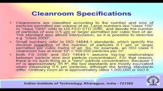
Additionally, the fabrication process necessitates a controlled environment known as a cleanroom, classified typically between Class 100 to 1000 to minimize the presence of airborne particulates. Precise control over multiple process parameters including temperature, pressure, and timing is also critical for producing reliable and efficient electronic devices.
Youtube Videos

Audio Book
Dive deep into the subject with an immersive audiobook experience.
Definition of Device Fabrication
Chapter 1 of 2
🔒 Unlock Audio Chapter
Sign up and enroll to access the full audio experience
Chapter Content
Process of transforming semiconductor materials into functional electronic components (transistors, diodes, ICs) using microfabrication techniques.
Detailed Explanation
Device fabrication refers to the series of processes that convert raw semiconductor materials into electronic components like transistors, diodes, and integrated circuits (ICs). This transformation is achieved through various advanced techniques collectively known as microfabrication. The microfabrication process involves precision engineering at a microscopic scale, allowing the creation of complex structures that are essential for modern electronic devices.
Examples & Analogies
Think of device fabrication like baking a cake. The semiconductor materials are like the raw ingredients (flour, sugar, eggs) that need to be mixed, shaped, and cooked properly to turn into a delicious cake. Just like each step in baking requires precision—measuring the ingredients, keeping track of the temperature, and timing the baking—device fabrication requires similar attention to detail to create functioning electronic components.
Key Requirements for Fabrication
Chapter 2 of 2
🔒 Unlock Audio Chapter
Sign up and enroll to access the full audio experience
Chapter Content
Cleanroom environment (Class 100-1000) and precise process control (temperature, pressure, timing).
Detailed Explanation
To successfully perform device fabrication, a cleanroom environment is essential. Cleanrooms are specially designed spaces that minimize contamination from dust, airborne microbes, or chemical vapors, maintaining a Class 100-1000 standard, which refers to the maximum allowable particles per cubic meter of air. Additionally, precise control of process parameters such as temperature, pressure, and timing is vital. Even slight deviations can affect the quality and functionality of the electronic devices being fabricated, making accuracy paramount.
Examples & Analogies
Imagine preparing a sterile operation room for surgery. Just as surgeons need a clean environment to ensure patient safety, device fabrication requires a contamination-free cleanroom to produce reliable electronic components. Moreover, it's similar to following a recipe precisely: if a chef doesn't measure the ingredients or control the cooking temperature accurately, the dish could turn out poorly, affecting the end result.
Key Concepts
-
Device Fabrication: The transformation of semiconductor materials into functional electronic components.
-
Cleanroom Environment: Controlled space essential to minimize contamination in the fabrication process.
-
Process Control: Maintaining optimal conditions such as temperature, pressure, and timing for successful device development.
Examples & Applications
Example 1: The fabrication of a MOSFET involves precise layering of gate oxides and controlled doping to form the device structure.
Example 2: Photolithography, a critical technique, is utilized to create patterns on semiconductor substrates by using photoresist materials.
Memory Aids
Interactive tools to help you remember key concepts
Rhymes
In the cleanroom we shall work, no dust will lurk, precise control, our goal's on a scroll!
Stories
Once in a land of tiny transistors, scientists gathered to build great resistors. They worked in a cleanroom, with tools in hand, ensuring each piece would perfectly stand.
Memory Tools
Remember the acronym C.P.T.: Cleanroom, Process Control, Temperature—all important for device fabrication.
Acronyms
Microdevices need
for Material
for Integrity
for Cleanroom
for Reliable Processes
and O for Optimal Conditions.
Flash Cards
Glossary
- Microfabrication
A set of techniques used to fabricate devices on the micro-scale, typically involving features that are micrometers in size.
- Cleanroom
A controlled environment with limited levels of pollutants used in manufacturing electronic devices to prevent contamination.
- Process Control
The method of controlling variables during fabrication processes, such as temperature, pressure, and timing to ensure the reliability of produced devices.
Reference links
Supplementary resources to enhance your learning experience.