
Apply Microfabrication Techniques to Fabricate Electronic Devices
Interactive Audio Lesson
Listen to a student-teacher conversation explaining the topic in a relatable way.
Overview of Device Fabrication
🔒 Unlock Audio Lesson
Sign up and enroll to listen to this audio lesson

Welcome, class! Today we're diving into the world of microfabrication. Can anyone tell me what device fabrication is?

Is it about making electronic devices?
Exactly! Device fabrication is the process of transforming semiconductor materials into electronic components like transistors and ICs. Why is a cleanroom important, think about it?

To avoid any dust or particles that could interfere, right?
Correct! Cleanrooms minimize contaminants which can degrade device performance. Let’s remember the term 'Class 100-1000' for the type of cleanroom we'll use.

How precise do we need to be?
Great question! We need precise control over temperature, pressure, and timing to achieve high-quality results.
So, to summarize, device fabrication involves cleanroom environments and precise process controls. Now let's move on to substrate preparation.
Substrate Preparation and Cleaning
🔒 Unlock Audio Lesson
Sign up and enroll to listen to this audio lesson

In the substrate preparation stage, we need to clean our wafers. What do we use for cleaning?

I think it's the RCA Clean?
Yes! The RCA Clean includes SC-1 and SC-2 steps. Can someone explain what SC-1 does?
SC-1 removes organics with NH₄OH, H₂O₂, and water.
Excellent! And what about SC-2?
It removes metals using HCl, H₂O₂, and water, right?
Correct! Then, we finish with an HF dip to remove native oxides. Why is that important?
To ensure good adhesion for the next layers!
Exactly! Let's remember these cleaning steps. Now, who can tell me what thin film deposition methods we use next?
Thin Film Deposition Methods
🔒 Unlock Audio Lesson
Sign up and enroll to listen to this audio lesson
Now we move to thin film deposition. Can anyone name a few methods?
Thermal oxidation and sputtering?
Perfect! Thermal oxidation is used to create SiO₂ layers. What thickness range do we typically use?
Anywhere from 5 to 500 nm?
Exactly! And what about LPCVD?
Used for Si₃N₄ and Poly-Si, usually 50 to 300 nm?
Yes, great job! And don’t forget the other materials like Al, Cu in PVD for interconnects. Let's summarize our thin film deposition methods.
Lithography and Etching
🔒 Unlock Audio Lesson
Sign up and enroll to listen to this audio lesson
Next, we need to pattern our films. What process do we use?
Photolithography!
Correct! The first step is spin-coating with a photoresist. What's the next one?
Soft bake?
Exactly! And after exposure comes the development stage. What happens here?
We immerse it in developer to create patterns!
True! Now onto etching—why do we use dry etching?
For better precision and selectivity?
Spot on! We can achieve selectivity greater than 20:1 for SiO₂ to Si. Let's recap the lithography and etching processes.
Doping and Metallization
🔒 Unlock Audio Lesson
Sign up and enroll to listen to this audio lesson
Finally, let's talk about doping. What method do we primarily use?
Ion implantation.
Correct! What are the common species used for n-type and p-type doping?
As⁺ for n-type and B⁺ for p-type?
Exactly! And don't forget we need to anneal afterward to activate the dopants. Now, what about metallization?
We deposit metals like Al or Cu and pattern them.
Yes! Then we anneal to enhance contacts. This wraps up our overview of microfabrication! Recap the key points we discussed today.
Introduction & Overview
Read summaries of the section's main ideas at different levels of detail.
Quick Overview
Standard
The section outlines the key steps and techniques used in microfabrication to convert semiconductor materials into functional electronic devices. It highlights the significance of precise environmental control and the specific processes that ensure successful device fabrication, including substrate preparation, lithography, etching, and doping.
Detailed
Detailed Summary
This section of Chapter 4 provides an overview of the microfabrication techniques essential for producing electronic devices such as transistors and integrated circuits. It begins by discussing the definition of device fabrication and the critical requirements, such as maintaining a cleanroom environment and precise process controls (temperature, pressure, and timing).
Key Stages of Fabrication:
- Substrate Preparation: Involves cleaning wafers using the RCA Standard Clean, which includes SC-1 and SC-2 washes for organic and metal removal, followed by an HF dip to remove native oxides.
- Thin Film Deposition: Techniques like thermal oxidation, LPCVD, and PVD are detailed with typical materials and applications.
- Patterning (Lithography): The photolithography process is explained, from spin-coating to development, ensuring fidelity in pattern transfer.
- Etching: The two types of etching are discussed—dry and wet—highlighting their chemistries and applications.
- Doping: Focuses on ion implantation for introducing dopants, with specific energy and dose parameters provided to achieve desired electrical properties.
- Metallization: Covers the process of depositing and patterning metals like aluminum or copper, concluding with annealing to form contacts.
Some challenges in process integration and advances in techniques, such as FinFET and 3D NAND fabrication, are also addressed, emphasizing the increasing complexity of integrated circuit fabrication as dimensions shrink.
Youtube Videos

Audio Book
Dive deep into the subject with an immersive audiobook experience.
Overview of Device Fabrication
Chapter 1 of 12
🔒 Unlock Audio Chapter
Sign up and enroll to access the full audio experience
Chapter Content
4.1 Overview of Device Fabrication
- Definition:
- Process of transforming semiconductor materials into functional electronic components (transistors, diodes, ICs) using microfabrication techniques.
- Key Requirements:
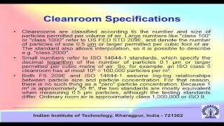
- Cleanroom environment (Class 100-1000)
- Precise process control (temperature, pressure, timing)
Detailed Explanation
This chunk introduces the concept of device fabrication. It explains that the process involves transforming raw semiconductor materials into actual working components used in electronic devices, such as transistors and integrated circuits. The definition highlights the significance of microfabrication techniques, which are specialized methods needed to create these tiny, precise structures. Additionally, it stresses two key requirements: firstly, a cleanroom environment is essential to avoid contamination, and it must meet specific cleanliness standards, generally referred to as Class 100-1000; secondly, the process control must be precise regarding factors like temperature, pressure, and timing to ensure high-quality outcomes.
Examples & Analogies
Think of device fabrication like baking a complex cake. Just as a clean kitchen and precise measurements are crucial for baking, a cleanroom and precise process control are necessary for creating electronic devices. If there’s too much dust or the oven is too hot, the final cake (or electronic device) won't turn out properly.
Step-by-Step Fabrication Process
Chapter 2 of 12
🔒 Unlock Audio Chapter
Sign up and enroll to access the full audio experience
Chapter Content
4.2 Step-by-Step Fabrication Process
4.2.1 Substrate Preparation
- Wafer Cleaning:
- RCA Standard Clean:
- SC-1: NH₄OH + H₂O₂ + H₂O (removes organics)
- SC-2: HCl + H₂O₂ + H₂O (removes metals)
- HF Dip: Removes native oxide (SiO₂)
Detailed Explanation
This chunk outlines the step-by-step fabrication process, starting with substrate preparation. Wafer cleaning is crucial because any contaminants on the surface can affect the performance of the electronic devices. The RCA Standard Clean outlines two key steps: SC-1, which involves a solution of ammonia, hydrogen peroxide, and water to remove organic materials, and SC-2, which uses hydrochloric acid, hydrogen peroxide, and water to eliminate metallic impurities. Finally, an HF dip is performed to remove any native oxide layer (SiO₂) present on the silicon wafer, ensuring a clean substrate for further processing.
Examples & Analogies
Imagine you’re preparing to paint a wall. Before you start, you need to clean the wall to remove any dust or grease. The RCA cleaning process is like that cleaning step—it ensures the wafer is spotless before any electronic features are added to it.
Thin Film Deposition Methods
Chapter 3 of 12
🔒 Unlock Audio Chapter
Sign up and enroll to access the full audio experience
Chapter Content
4.2.2 Thin Film Deposition
| Method | Materials | Typical Thickness | Application |
|---|---|---|---|
| Thermal Oxidation | SiO₂ | 5–500 nm | Gate dielectric |
| LPCVD | Si₃N₄, Poly-Si | 50–300 nm | Masking layers, gates |
| PVD (Sputtering) | Al, Cu, TiN | 100 nm–1 μm | Interconnects, electrodes |
Detailed Explanation
In this chunk, the various methods of thin film deposition are presented. Thin films are essential layers applied to the semiconductor wafer for different functionalities. Thermal oxidation grows silicon dioxide (SiO₂) layers, which typically range from 5 to 500 nm and serve as gate dielectrics in transistors. Low-Pressure Chemical Vapor Deposition (LPCVD) is highlighted for depositing materials like silicon nitride and polysilicon, while Physical Vapor Deposition (PVD), including sputtering, is used to lay down metals such as aluminum and copper for interconnections and electrodes. Each method has its specific material types, thicknesses, and applications.
Examples & Analogies
Imagine applying layers of frosting to a cake. Each layer has a specific purpose – some add flavor while others provide decoration or structural support. Similarly, each thin film layer in microfabrication has a unique role—some insulate, while others conduct electricity.
Patterning (Lithography)
Chapter 4 of 12
🔒 Unlock Audio Chapter
Sign up and enroll to access the full audio experience
Chapter Content
4.2.3 Patterning (Lithography)
- Photolithography Process:
- Spin-coating: Apply photoresist (e.g., AZ 5214) at 3000–5000 RPM.
- Soft Bake: 90–120°C for 60 sec.
- Exposure: UV light (365–436 nm) through a photomask.
- Development: Immerse in developer (e.g., MF-319) for 30–60 sec.
Detailed Explanation
This section describes the photolithography process used for patterning the surfaces of wafers. The process begins with spin-coating a photoresist substance, which is spread evenly on the wafer's surface at high speeds (3000-5000 RPM). After coating, a soft bake is performed to set the photoresist. The exposure step involves shinning ultraviolet light through a photomask that contains the desired pattern, transferring this pattern onto the photoresist. Finally, the development step involves immersing the wafer in a developer solution, which removes either the exposed or unexposed areas of the photoresist, depending on the type used.
Examples & Analogies
Think of photolithography like creating a stencil for spray painting. You first apply a light adhesive (the photoresist), then place the stencil (photomask) over it and spray (expose to UV light) before carefully peeling it away to leave behind a patterned design on the surface.
Etching Techniques
Chapter 5 of 12
🔒 Unlock Audio Chapter
Sign up and enroll to access the full audio experience
Chapter Content
4.2.4 Etching
- Dry Etching (RIE):
- Chemistry: CF₄/O₂ for SiO₂, Cl₂/BCl₃ for metals.
- Selectivity: >20:1 for SiO₂/Si.
- Wet Etching:
- SiO₂: Buffered HF (6:1 NH₄F:HF).
- Si: KOH (anisotropic, 54.7° sidewalls).
Detailed Explanation
This chunk delves into etching, which is a crucial step for defining patterns on semiconductor wafers. Two primary etching methods are highlighted: dry etching and wet etching. Reactive Ion Etching (RIE) is a dry etching process that uses gases like CF₄ and O₂ to etch silicon dioxide and Cl₂/BCl₃ for metals. It has high selectivity, meaning it can effectively distinguish between SiO₂ and silicon with a ratio of over 20:1. Wet etching is also important, with buffered HF used for etching silica and KOH for silicon, which yields specific sidewall angles critical for device performance.
Examples & Analogies
Etching can be likened to carving a design into a pumpkin. If you apply a carving tool (etching method) carefully, you can create intricate details while leaving the pumpkin's structure intact. Similarly, etching precisely removes parts of a layer without damaging the underlying material.
Doping Techniques
Chapter 6 of 12
🔒 Unlock Audio Chapter
Sign up and enroll to access the full audio experience
Chapter Content
4.2.5 Doping
- Ion Implantation:
- Species: As⁺ (n-type), B⁺ (p-type).
- Energy: 10–200 keV, Dose: 1e11–1e16 ions/cm².
- Annealing:
- 900–1100°C in N₂ to activate dopants.
Detailed Explanation
Doping is a critical process that alters the electrical properties of semiconductor materials. This chunk explains ion implantation, where dopant ions (such as arsenic for n-type and boron for p-type) are introduced into the semiconductor substrate at various energy levels (10-200 keV). The dose, or number of ions applied per cm², is carefully controlled to achieve the desired electrical characteristics. After implantation, an annealing step (in which the wafer is heated in a nitrogen atmosphere at 900-1100°C) is performed to activate the dopants, allowing them to effectively alter the conductivity of the treated area.
Examples & Analogies
Imagine you’re adding a tiny amount of salt to improve the flavor of a large pot of soup. The salt represents the dopants in doping; just as adding salt changes the soup’s taste, doping modifies the semiconductor's electrical properties to meet specific needs.
Metallization Process
Chapter 7 of 12
🔒 Unlock Audio Chapter
Sign up and enroll to access the full audio experience
Chapter Content
4.2.6 Metallization
- Process Flow:
- Deposit Al/Cu via sputtering.
- Pattern using lithography + RIE.
- Anneal (400°C, 30 min) for contact formation.
Detailed Explanation
This section covers the metallization process, which is essential for creating interconnections between different components in an electronic device. The first step involves depositing metals like aluminum or copper onto the wafer using sputtering techniques. The deposited layer is then patterned through lithography and reactive ion etching to define the desired circuitry. Finally, an annealing step at 400°C for 30 minutes helps to form stable electrical contacts by promoting the bonding between the metal and the underlying semiconductor material.
Examples & Analogies
Consider metallization as creating electrical pathways on a circuit board. Just like you’d draw tracks with a pen to connect different points on a board for a project, metallization lays down metal pathways to connect the various parts of a semiconductor device, allowing for communication and functionality.
Example: Fabricating a MOSFET
Chapter 8 of 12
🔒 Unlock Audio Chapter
Sign up and enroll to access the full audio experience
Chapter Content
4.3 Example: Fabricating a MOSFET
4.3.1 Process Flow
- Substrate: p-type Si wafer.
- Gate Oxide: Grow 10 nm SiO₂ (dry oxidation at 900°C).
- Gate Electrode: Deposit + pattern 200 nm poly-Si.
- Source/Drain: Implant As⁺ (50 keV, 5e15/cm²).
- Contacts: Sputter + pattern Al.
Detailed Explanation
In this chunk, a specific example of fabricating a Metal-Oxide-Semiconductor Field-Effect Transistor (MOSFET) is outlined. The process begins with a p-type silicon wafer as the substrate. Then, a 10 nm thick layer of silicon dioxide is grown as the gate oxide through dry oxidation at 900°C. Following that, a layer of poly-silicon is deposited and patterned to form the gate electrode. The source and drain regions are formed by implanting arsenic ions into the silicon wafer. Finally, contacts are created by sputtering and patterning aluminum, connecting the MOSFET to the rest of the circuit.
Examples & Analogies
Building a MOSFET is akin to constructing a multi-story building. Each step represents a phase of construction: laying the foundation (substrate), adding floors (gate oxide), placing windows (gate electrode), installing utilities (source/drain), and finally connecting everything to a power source (contacts).
Critical Parameters in MOSFET Fabrication
Chapter 9 of 12
🔒 Unlock Audio Chapter
Sign up and enroll to access the full audio experience
Chapter Content
4.3.2 Critical Parameters
| Parameter | Target Value | Measurement Method |
|---|---|---|
| Gate oxide thickness | 10 ± 0.5 nm | Ellipsometry |
| Channel length | 180 nm | SEM |
| Threshold voltage | 0.3–0.5 V | I-V characterization |
Detailed Explanation
This chunk identifies critical parameters that must be measured during the fabrication of a MOSFET to ensure proper functionality. The thickness of the gate oxide layer is targeted at 10 nm with a permissible variation of ±0.5 nm, determined by ellipsometry, a technique that measures the change in polarization of light. The channel length of the MOSFET is specified as 180 nm, measured using Scanning Electron Microscopy (SEM). Finally, the threshold voltage, which is crucial for device operation, is expected to be in the range of 0.3 to 0.5 V and is characterized through current-voltage (I-V) testing.
Examples & Analogies
Think of critical parameters in MOSFET fabrication like specifications that must be met when building a car. Just as a car must have a certain horsepower, fuel efficiency, and safety ratings to be deemed reliable, the MOSFET must meet specific parameters to function effectively in electronic circuits.
Process Integration Challenges
Chapter 10 of 12
🔒 Unlock Audio Chapter
Sign up and enroll to access the full audio experience
Chapter Content
4.4 Process Integration Challenges
- Alignment Errors: <±50 nm overlay accuracy for <100 nm nodes.
- Defect Density: <0.1 defects/cm² for high yield.
- Stress Control: Compressive/Tensile stress in films affects device reliability.
Detailed Explanation
This chunk discusses the challenges associated with integrating the various fabrication processes to produce reliable devices. Alignment errors are a significant issue; at feature sizes below 100 nm, the overlay accuracy must remain within ±50 nm to ensure proper functioning. Additionally, defect density must be minimized, with an acceptable level being less than 0.1 defects per cm² to maintain high yield rates. Lastly, controlling stress within the films is crucial, as both compressive and tensile stresses can lead to reliability issues in the final electronic devices.
Examples & Analogies
Think of building a complex jigsaw puzzle. Each piece must fit perfectly together for the final image to be coherent. If there’s a misalignment or if pieces have flaws (defects), the whole picture (device performance) will be compromised.
Advanced Techniques in Microfabrication
Chapter 11 of 12
🔒 Unlock Audio Chapter
Sign up and enroll to access the full audio experience
Chapter Content
4.5 Advanced Techniques
- FinFET Fabrication:
- Uses double-patterning lithography for 3D fins.
- 3D NAND:
- Vertical stacking of memory cells with >64 layers.
Detailed Explanation
This chunk highlights some advanced techniques in microfabrication. FinFET (Fin Field-Effect Transistor) fabrication is discussed, which employs double-patterning lithography to create three-dimensional fins that enhance performance and reduce leakage current in transistors. The section also introduces 3D NAND technology, where memory cells are stacked vertically in layers exceeding 64, significantly increasing storage capacity while maintaining a small footprint.
Examples & Analogies
Consider FinFETs like constructing multi-level parking garages instead of traditional lots. Just as a vertical design maximizes parking space efficiency, FinFETs optimize space on a chip to improve performance. Similarly, the 3D NAND technology can be compared to high-rise buildings that efficiently utilize vertical space, allowing for more apartments (data storage) in a smaller area.
Summary of Device Fabrication
Chapter 12 of 12
🔒 Unlock Audio Chapter
Sign up and enroll to access the full audio experience
Chapter Content
4.6 Summary
- Device fabrication requires sequential deposition, patterning, and etching steps.
- Key metrics: Feature size, doping uniformity, and interfacial quality.
- Process integration becomes exponentially complex at smaller nodes (<28 nm).
Detailed Explanation
This chunk summarizes the essential points of the device fabrication process. It emphasizes that the overall procedure involves a series of sequential steps involving the deposition of materials, patterning them, and then etching away unwanted areas. Three critical metrics are pointed out: feature size, which affects the density of devices; doping uniformity, which influences performance consistency; and interfacial quality, which affects the reliability of connections between different layers. Lastly, the summary notes that as technology advances and feature sizes shrink below 28 nm, the complexities of process integration increase significantly.
Examples & Analogies
Think of summarizing a complex process like making a movie. Each step—from scriptwriting (depiction), casting (patterning), to filming (etching)—is crucial for the final product. Similarly, the summarized points highlight the importance of each stage in device fabrication, where precision and clarity play a significant role in the success of the outcome.
Key Concepts
-
Device Fabrication: The transformation of semiconductor materials into functional electronic components.
-
Cleanroom Environment: A controlled space minimizing contaminants to ensure high-quality device fabrication.
-
Substrate Preparation: The initial stage involves cleaning wafers to remove impurities for enhanced adhesion.
-
Thin Film Deposition: Various methodologies (Thermal, LPCVD, PVD) to create thin films required for device functionality.
-
Patterning: Lithographic techniques for accurately defining device geometries through light exposure.
-
Doping: Introduction of dopants to modify semiconductor properties, crucial for the electrical behavior of devices.
-
Metallization: Final layering of metal to create connections, necessitating precise patterning and annealing.
Examples & Applications
Using thermal oxidation to grow 10 nm SiO₂ for gate oxide in MOSFET fabrication.
Applying photolithography to define features on an integrated circuit with precision.
Utilizing ion implantation to introduce As⁺ and B⁺ for n-type and p-type doping in semiconductors.
Memory Aids
Interactive tools to help you remember key concepts
Rhymes
In a cleanroom 100 to 1000, we craft, / Wafers in layers, thin films we draft.
Stories
Imagine a tiny factory where every step is carefully controlled. Workers scrub the floors (cleanroom), layer the cakes (thin films), and use stencils to decorate (lithography), ensuring the cake looks perfect to everyone at the party (the devices).
Memory Tools
Remember 'SLEAD' for the order of processes: Substrate preparation, Lithography, Etching, Doping, Metallization.
Acronyms
DAMP for Doping, Annealing, Metallization, Patterning.
Flash Cards
Glossary
- Microfabrication
Techniques to create small structures on a semiconductor for electronic devices.
- Cleanroom
Controlled environment for manufacturing to minimize contamination.
- Substrate
Base material that supports the deposition of thin films.
- Lithography
Process to pattern materials using light or other radiation.
- Doping
Introducing impurities into semiconductors to modify electrical properties.
- Metallization
The process of depositing metal layers for electrical connections.
Reference links
Supplementary resources to enhance your learning experience.