
Analog Electronic Circuits
Enroll to start learning
You’ve not yet enrolled in this course. Please enroll for free to listen to audio lessons, classroom podcasts and take practice test.
Interactive Audio Lesson
Listen to a student-teacher conversation explaining the topic in a relatable way.
Understanding Common Collector Amplifiers
🔒 Unlock Audio Lesson
Sign up and enroll to listen to this audio lesson

Welcome, everyone! Today we’ll discuss common collector amplifiers and how biasing affects their performance. Can anyone explain what a common collector amplifier is?

Is it a type of amplifier where the output is taken from the emitter?
Exactly! The output is connected to the emitter. Now, why do you think biasing is crucial for this type of amplifier?

I think it’s important to keep the transistor in the active region, right?
That's correct! We need to maintain the collector current and voltage in certain ranges. So, can anyone summarize how we derive the biasing conditions?

We consider the DC supply and the expected collector current to find the voltage across various resistances in the circuit.
Well done! Remember, proper biasing ensures stable performance across the amplifier’s operational range.
Calculating Voltage Gain and Impedance
🔒 Unlock Audio Lesson
Sign up and enroll to listen to this audio lesson

Now let's calculate the voltage gain in our common collector setup. What do we expect the gain to be?

It should be close to 1, right?
Exactly! Now, can you recall how we calculate it mathematically?
I believe it involves transconductance and output resistance?
Correct again! Specifically, the formula includes $A_v = rac{g_m imes r_o}{g_m + rac{1}{r_π}}$. Now, what about input impedance?
The input impedance is usually high because of the base resistor and the transistor's properties.
Perfect! High input impedance is desirable to minimize loading effects on the previous stage.
Impact of Parasitic Components
🔒 Unlock Audio Lesson
Sign up and enroll to listen to this audio lesson
Now, let's discuss parasitic capacitances and their significant impact on amplifier behavior. What parasitic components can you think of?
There are base-collector capacitances and load capacitances.
Exactly! These capacitances can limit the bandwidth of the amplifier. Can anyone explain how we calculate the upper cutoff frequency?
We take the output resistance and multiply by the load capacitance, right?
Yes, and it’s given by $f_{upper} = rac{1}{2 ext{π}R_{out}C_{load}}$. Remember, larger capacitances push the frequency response lower.
So keeping capacitance low is important to retain high frequency responses!
Exactly! You’ve got it.
Introduction & Overview
Read summaries of the section's main ideas at different levels of detail.
Quick Overview
Standard
The section details numerical examples related to common collector and common drain amplifiers, emphasizing the importance of design parameters such as voltage gain, input and output impedance, and loading effects. It explains how these factors are influenced by circuit biasing and parasitic capacitances, ultimately impacting the amplifier's frequency response.
Detailed
Detailed Summary
This section continues the examination of common collector and common drain amplifiers through practical numerical examples and design guidelines. It begins by reiterating the importance of key parameters, including voltage gain, input and output impedance, and their dependence on circuit conditions such as biasing and parasitic capacitances.
The section outlines a specific example, starting with proposed biasing voltages and the impact of thermal voltage, which reveals how the ideal bias conditions influence the performance metrics of the amplifier. Following this, detailed calculations are performed to derive the operating point, illustrating how to calculate parameters like the collector current and emitter voltage.
The text goes on to explain small signal parameters, including transconductance ($g_m$), base-emitter impedance ($r_π$), and output resistance ($r_o$), providing insights into their formulas and calculations. Moreover, it highlights the expected voltage gain, input resistance, and output impedance, all aiming for optimal performance within the determined design constraints.
The implications of loading effects are also explored, such as how changes in load capacitance impact frequency response. Finally, the text illustrates the approach for determining upper cutoff frequency and emphasizes how practical circuit considerations, like source resistance, influence amplifier design and functionality.
Youtube Videos

Audio Book
Dive deep into the subject with an immersive audiobook experience.
Introduction to Common Collector and Common Drain Amplifiers
Chapter 1 of 6
🔒 Unlock Audio Chapter
Sign up and enroll to access the full audio experience
Chapter Content
So today, we are going to continue the discussion on Common Collector and Common Drain Amplifiers.
So, the outline of today’s presentation, it is given in the next slide. What we are going to do today it is primarily, we will be focusing on numerical examples and design guidelines of common collector and common drain amplifiers.
Detailed Explanation
In this introduction, the focus is set on continuing the discussion about Common Collector and Common Drain amplifiers, two important configurations in analog electronics. The aim is to present numerical examples and design guidelines related to these amplifiers, building on the knowledge gained from previous discussions.
Examples & Analogies
Think of these amplifiers as different types of engines in vehicles. Just like how different engines are suitable for different types of vehicles, Common Collector and Common Drain amplifiers are suited for specific applications in electronic circuits, and understanding their designs helps optimize their performance.
Understanding Biasing and Circuit Components
Chapter 2 of 6
🔒 Unlock Audio Chapter
Sign up and enroll to access the full audio experience
Chapter Content
In fact, I should say that V BB is making a bias at the base terminal and then we do have the DC supply of 10 V. So, V BB is given here, it is 6 V.
And then we assume that the thermal equivalent voltage it is 26 mV; then, we are also considering that load capacitance connected at the output node; C L and its value it is say 100 pF.
Detailed Explanation
This part discusses the biasing setup for the amplifier. 'V BB' represents the voltage applied to provide the necessary bias at the base terminal of the transistor. A DC supply of 10 V is connected to the circuit with V BB set to 6 V. The thermal equivalent voltage is a constant value used in calculations, and a load capacitance of 100 pF is included to study how it affects circuit behavior.
Examples & Analogies
Imagine you are trying to start a car engine. The voltage supplied by the battery is like the DC supply for the amplifier. Just as you need a good start to keep the engine running smoothly, biasing the amplifier helps it function correctly in the desired operating range.
Finding the Operating Point
Chapter 3 of 6
🔒 Unlock Audio Chapter
Sign up and enroll to access the full audio experience
Chapter Content
So, if I analyze this circuit and if I consider bias current it is, 0.5 mA it is given to us. So, we can say that the collector current, it is also approximately equal to the emitter current. So, that is 0.5 mA,... So, from this one we can see that the transistor, it is in active region of operation.
Detailed Explanation
To find the operating point of the transistor, we consider the bias current, which is given as 0.5 mA. This current flows through the transistor, and because of the nature of bipolar junction transistors, the collector current is nearly equal to the emitter current. By analyzing the voltage drops across the circuit components, we can confirm that the transistor is in its active region, which is necessary for proper amplification.
Examples & Analogies
Consider a train that needs to be on the right track (active region) to function correctly – if it's not in the right place, it won't go anywhere. Similarly, ensuring the transistor is in the active region allows it to amplify signals effectively.
Calculating Small Signal Parameters
Chapter 4 of 6
🔒 Unlock Audio Chapter
Sign up and enroll to access the full audio experience
Chapter Content
So, let me start going to the operating point first...let us start with g m and you may recall its expression in terms of the quotient current, it is collector current divided by thermal equivalent voltage.
Detailed Explanation
Analyzing small-signal parameters is an important step in amplifier design. The transconductance 'g m' relates the change in output current to the change in input voltage and is calculated using the collector current divided by the thermal voltage. This small-signal model helps design the circuit for desired characteristics like gain and bandwidth.
Examples & Analogies
Think of driving a car where you need precise control of the accelerator (input voltage) to adjust the speed (output current). Just like in driving, understanding and calculating small signal parameters enables you to manage how the amplifier responds to input signals.
Calculating Voltage Gain and Impedances
Chapter 5 of 6
🔒 Unlock Audio Chapter
Sign up and enroll to access the full audio experience
Chapter Content
Let me clear the space and then again. Let me start with the voltage gain, small signal voltage gain A = v o / v in. So, we may see that this is connected to AC ground.
Detailed Explanation
The voltage gain of the amplifier, denoted as A, is calculated by the ratio of output voltage to input voltage. The setup assumes one terminal is connected to AC ground. Understanding how the gain is derived from small signal parameters helps assess how effectively the amplifier can strengthen signals.
Examples & Analogies
Imagine using a microphone to amplify your voice. The small amount of sound (input) gets transformed into a loud sound (output) that is proportional to your voice. The voltage gain acts similarly, quantifying how much the input signal is magnified.
Upper Cutoff Frequency Calculation
Chapter 6 of 6
🔒 Unlock Audio Chapter
Sign up and enroll to access the full audio experience
Chapter Content
So, we can say that the upper cutoff frequency now... let me use a different color should see R o / C L.
Detailed Explanation
The upper cutoff frequency is a critical concept in amplifier design, indicating the maximum frequency at which the amplifier can operate effectively without significant loss of gain. This frequency is calculated using the output resistance and load capacitance. Understanding this aspect ensures that the amplifier can handle the frequency of the signals it is meant to process.
Examples & Analogies
Consider a water pipe that can only allow a certain amount of water flow before it gets blocked (loses efficiency). Similarly, knowing the upper cutoff frequency helps in understanding how fast or slow the amplified signals can flow through the amplifier.
Key Concepts
-
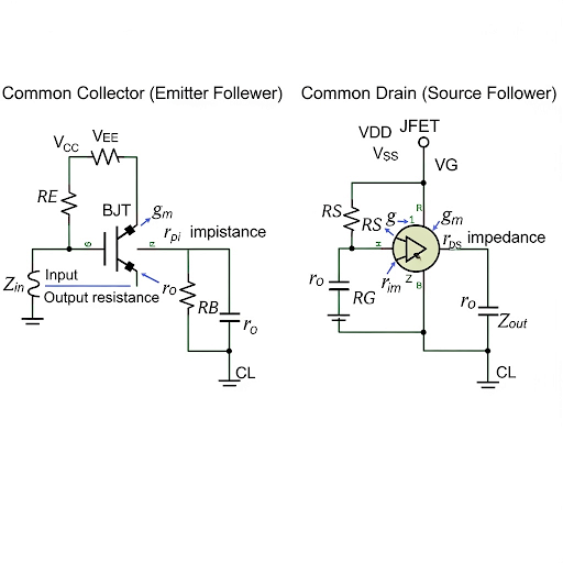
Common Collector Configuration: Key amplifier configuration offering high input impedance and the role of biasing.
-
Voltage Gain Characteristics: Importance of low gain close to 1 for common collector amplifiers.
-
Parasitics Influence: Understanding how parasitic capacitances can affect the frequency response of amplifiers.
Examples & Applications
Example of calculating the voltage gain in a common collector amplifier configuration given specific bias conditions and load capacitance values.
Exploring the impact of varying the load capacitance on the upper cutoff frequency of a common collector amplifier.
Memory Aids
Interactive tools to help you remember key concepts
Rhymes
In a collector configuration, the output's through the emitter, gains close to one, it's a helper, not a hitter.
Stories
Imagine a football game where the wide receiver is always at the goal line, catching passes that barely cross the line—this represents the low gain of a common collector amplifier.
Memory Tools
Remember 'COLL' for Common Collector: Close to one (gain), Output on emitter, Load capacitors lower frequency.
Acronyms
C.C.A = Common Collector Amplifier
Keeps current Constant
Gain near One.
Flash Cards
Glossary
- Common Collector Amplifier
An amplifier configuration where the output is taken from the emitter terminal, providing voltage buffering and high input impedance.
- Biasing
The process of applying DC voltages to transistors to establish proper operating conditions.
- Voltage Gain
The ratio of output voltage to input voltage, often denoted as Av.
- Impedance
A measure of how much a circuit resists the flow of electric current, calculated as a complex ratio of voltage to current.
- Parasitic Capacitance
Unintended capacitances that occur within electronic components due to their physical construction, often affecting circuit performance.
- Upper Cutoff Frequency
The frequency at which the gain of an amplifier drops to -3 dB from its maximum value.
Reference links
Supplementary resources to enhance your learning experience.