
Next Circuit with Practical Source Resistance
Enroll to start learning
You’ve not yet enrolled in this course. Please enroll for free to listen to audio lessons, classroom podcasts and take practice test.
Interactive Audio Lesson
Listen to a student-teacher conversation explaining the topic in a relatable way.
Introduction to Common Collector Amplifiers
🔒 Unlock Audio Lesson
Sign up and enroll to listen to this audio lesson

Today, we're exploring common collector amplifiers. Can anyone tell me what a common collector configuration is?

Isn't it when the collector is common to both input and output?
Exactly! It's often used for impedance matching. One key goal is to achieve a voltage gain close to 1. Let's remember that with the tip 'gain is plain', which hints at minimal gain in this configuration.

How do we calculate the output impedance?
Good question! The output impedance calculation involves resistance values and conductance terms. We typically use the formula involving small signal parameters. Let's keep that in mind with the mnemonic 'Z = G-inverse'.
Calculating Voltage Gain
🔒 Unlock Audio Lesson
Sign up and enroll to listen to this audio lesson

Now let’s calculate the voltage gain for our common collector circuit. Can anyone remind me how we express voltage gain mathematically?

Is it the ratio of output to input voltage?
Correct! The formula is A = V_out / V_in. In the case of common collector, we're looking for A to be close to 1. Use the hint 'Almost the same' to help recall its function.

What factors affect voltage gain in practical scenarios?
Excellent inquiry! Factors include the beta of the transistor, the load resistance, and source resistance. Let’s memorize: 'Beta is key, load must agree'.
Understanding Input and Output Impedance
🔒 Unlock Audio Lesson
Sign up and enroll to listen to this audio lesson
Next, we will explore input and output impedance. Why do you think input impedance is crucial in amplifier circuits?
So we can prevent loading effects on the previous stage?
Precisely! You want a high input impedance. Remember the acronym 'HIP' for High Input Power. How do we calculate it?
Is it based on small signal parameters?
Exactly! We usually consider both the intrinsic resistance of the components and the small signal representation. Remember: 'Small signal, big picture'!
Evaluating the Impact of Source Resistance
🔒 Unlock Audio Lesson
Sign up and enroll to listen to this audio lesson
Let's shift gears to source resistance. How does introducing source resistance change our circuit's performance?
It could lower the voltage at the base, right?
Yes, spot on! This change affects operating points and can lead to altered gains. To remember this, use the phrase 'Resistance rules'.
What about the output frequency response?
Great point! An increased source resistance may decrease bandwidth. I suggest using the shortcut 'Bandwidth beneath Resistance'.
Introduction & Overview
Read summaries of the section's main ideas at different levels of detail.
Quick Overview
Standard
In this section, we delve into the behavior of common collector and common drain amplifiers, emphasizing numerical examples that illustrate the impact of source resistance. Key parameters such as voltage gain, input/output impedance, and upper cutoff frequency are calculated to enhance understanding.
Detailed
Detailed Summary
This section elaborates on the analysis and design of common collector and common drain amplifiers using numerical examples. The discussion begins with an ideal case that includes a common collector amplifier with various parameters defined, such as bias voltage, load capacitance, thermal equivalent voltage, and device parameters like B2 (beta) and Early voltage.
Crucially, students learn how to compute significant amplifier metrics, including voltage gain, input and output impedance, and the upper cutoff frequency. The analysis focuses on creating a working knowledge of these parameters while emphasizing that performance optimizations should target minimal attenuation (voltage gain close to 1) and achieving high input and low output impedance. The underlying theories are tested through calculations based on given parameters, leading to an understanding of how practical elements like source resistance affect the circuit's behavior.
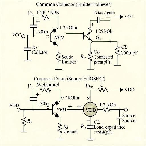
Towards the end, the concept of how altered source resistance alters the operating point and output characteristics is affirmed through a comparative evaluation of scenarios with and without practical source resistance.
Youtube Videos

Audio Book
Dive deep into the subject with an immersive audiobook experience.
Introduction to Practical Source Resistance
Chapter 1 of 5
🔒 Unlock Audio Chapter
Sign up and enroll to access the full audio experience
Chapter Content
In the next slide, it is basically the same circuit except, here we are considering the source resistance R different from different from 100 k. So, if you see this circuit if you analyze this circuit with the bias current of say 0.5 mA and then if you try to analyze what will be the operating point.
Detailed Explanation
In this chunk, we are looking at the introduction of a practical source resistance into the amplifier circuit. The practical source resistance is a crucial consideration because it affects the voltage drop across components and the overall behavior of the circuit. By adjusting the source resistance, we can analyze how the amplifier functions under realistic conditions as opposed to ideal ones, which helps us understand the importance of this parameter in circuit design.
Examples & Analogies
Imagine you're trying to fill a glass with water. If the faucet has a high pressure, the water flows quickly. But if there's a blockage (like a practical source resistance), the flow rate reduces, and it takes longer to fill the glass. This is similar to how practical source resistance can limit the current flow in an amplifier circuit.
Operating Point with Source Resistance
Chapter 2 of 5
🔒 Unlock Audio Chapter
Sign up and enroll to access the full audio experience
Chapter Content
So we do have at the base we do have the 6 V of this V_BB, and then we do have the R_S and then base to emitter we do have a voltage drop. So, so I should say I am just circling it to indicate that this is representing V_BE(on).
Detailed Explanation
In this segment, we determine the operating point of the amplifier considering the source resistance. The base voltage is initially set at 6 V. When current flows through the source resistance (R_S), there is a voltage drop due to the current flowing through it, which affects the base voltage. This means we need to recalculate the base-emitter voltage considering the drop, as it changes the conditions under which the transistor operates.
Examples & Analogies
Think of a car trying to go uphill (transistor working). If the car has more weight (source resistance), it struggles more, and it slows down (drops voltage). This situation forces the car to adjust its acceleration (operating point) according to the incline (circuit bias conditions).
Maintaining the Same Small Signal Parameters
Chapter 3 of 5
🔒 Unlock Audio Chapter
Sign up and enroll to access the full audio experience
Chapter Content
Note that even though the voltage here it is different from significantly different from 6 V bias here due to finite value of this source resistance. But since we do have the bias current here it is ideal quote and non-quote ideal of the same value of 0.5 mA the collector current and base current hardly gets affected.
Detailed Explanation
Despite the changes in base voltage due to source resistance, the bias current remains constant at 0.5 mA, meaning the collector and base currents also remain unaffected. This indicates that the small signal parameters like the transconductance and output resistance stay the same, which in turn shows that the overall performance of the amplifier remains predominantly unchanged even with practical source resistance.
Examples & Analogies
Imagine you're baking cookies and you switch ovens but keep the temperature settings the same. Although the ovens may behave slightly differently, if you maintain the right temperature (bias current), your cookie recipes (small signal parameters) will still turn out fine.
Calculating Output Impedance
Chapter 4 of 5
🔒 Unlock Audio Chapter
Sign up and enroll to access the full audio experience
Chapter Content
So now, you may recall that at this point if we give a give a stimulus of say v_x in the small signal equivalent circuit; then if we try to calculate what is the corresponding i_x.
Detailed Explanation
In this chunk, the discussion focuses on calculating the output impedance while considering source resistance. We have to analyze the circuit by providing a small signal voltage (v_x) and evaluating how it translates to the corresponding output current (i_x). The output impedance is influenced by the source resistance and the other impedance parameters of the circuit. This helps us understand how the output of the circuit will behave under variations in load and input signals.
Examples & Analogies
This can be likened to how the responsiveness changes in a water pressure system when you add a tap (representing the source resistance). If the tap is partially closed, it affects how much water (output) can flow out, and this is what we’re analyzing in terms of the circuit’s output behavior.
Understanding Upper Cutoff Frequency
Chapter 5 of 5
🔒 Unlock Audio Chapter
Sign up and enroll to access the full audio experience
Chapter Content
So the upper cutoff frequency of course, it will be defined by whichever is minimum.
Detailed Explanation
In this portion, the concept of upper cutoff frequency is explained. The upper cutoff frequency defines the maximum frequency at which the amplifier can respond. It's determined by the interactions of various impedances in the circuit, including the source resistance and capacitance. The minimum of these cutoff frequencies sets the bandwidth of the amplifier, thereby defining the range of frequencies it can effectively amplify.
Examples & Analogies
Consider a music equalizer that can adjust sound frequencies to desirable levels. If one frequency band is cut off more than others, it limits the range of sound you can enjoy, similar to how the upper cutoff frequency limits the amplifier's response.
Key Concepts
-
Common Collector Amplifier: Provides high input impedance and low output impedance.
-
Voltage Gain: Desired to be close to 1 for common collector configurations.
-
Source Resistance: Affects biasing and needs to be accounted for in real circuits.
Examples & Applications
In a common collector amplifier with a bias current of 0.5 mA, a base voltage of 6V leads to an emitter voltage of 5.4 V, maintaining the transistor in active region.
When calculating the upper cutoff frequency of an amplifier with a load capacitance of 100 pF and practical source resistance, the frequency may adjust downwards from an ideal scenario.
Memory Aids
Interactive tools to help you remember key concepts
Rhymes
Gain is plain, common collector’s main.
Stories
Imagine a friendly amplifier sharing, balancing inputs and outputs without caring.
Memory Tools
Z = G-inverse helps you remember output impedance calculations.
Acronyms
HIP
High Input Power
to remember why input impedance is important.
Flash Cards
Glossary
- Common Collector Amplifier
A type of amplifier configuration that provides a high input impedance and low output impedance, commonly used for impedance matching.
- Voltage Gain
The ratio of the output voltage to the input voltage in an amplifier, indicating how much the signal is amplified.
- Source Resistance
The resistance in series with the source voltage that can impact the voltage delivered to the amplifier's input.
- Upper Cutoff Frequency
The frequency above which the output power of the amplifier drops significantly, defining the bandwidth.
- Beta (β)
The current gain of the transistor, defined as the ratio of collector current to base current.
Reference links
Supplementary resources to enhance your learning experience.