
Common Collector Amplifier Example
Enroll to start learning
You’ve not yet enrolled in this course. Please enroll for free to listen to audio lessons, classroom podcasts and take practice test.
Interactive Audio Lesson
Listen to a student-teacher conversation explaining the topic in a relatable way.
Introduction to Common Collector Amplifier
🔒 Unlock Audio Lesson
Sign up and enroll to listen to this audio lesson

Today, we’ll explore the common collector amplifier, known for its ability to provide a high input impedance and low output impedance. Can anyone tell me what these properties mean in a circuit?

High input impedance means it won't load down the source, right?
Exactly, and low output impedance allows it to drive loads effectively without significant signal loss.

So, it’s useful for matching different stages in a circuit?
Correct! This makes it a favorite for many applications including buffers. Now, let's look at an example to see these principles in action.
Analyzing a Numerical Example
🔒 Unlock Audio Lesson
Sign up and enroll to listen to this audio lesson

Let’s analyze a common collector amplifier where we are given a DC supply of 10V and a biasing voltage of 6V. Who can recall how to determine the emitter voltage from these values?

The emitter voltage is the base voltage minus the base-emitter voltage drop!
Exactly! The base-emitter drop is typically around 0.6V, giving us an emitter voltage of 5.4V.

And how do we make sure the transistor is operating in the active region?
Good question! We need to ensure the collector voltage is higher than the emitter voltage. In this case, with 10V at the collector, it’s definitely in the active region.
Calculating Voltage Gain and Impedances
🔒 Unlock Audio Lesson
Sign up and enroll to listen to this audio lesson
Now that we have determined our operating point, let’s calculate the small signal voltage gain. Does anyone remember the formula for voltage gain in a common collector circuit?
It involves the transconductance and output resistance?
Exactly! The formula is A = (gm * Ro) / (1 + gm * Rs), where gm is transconductance and Ro is output resistance. Let’s substitute our values and calculate.
What about the input impedance?
The input impedance R_in can be found using the equation R_in = (β + 1)*re. Remember re can be calculated from the collector current.
So we get a high impedance value, which is beneficial for amplifiers!
Well summarized! This is crucial for ensuring signal integrity.
Introduction & Overview
Read summaries of the section's main ideas at different levels of detail.
Quick Overview
Standard
In this section, we explore the common collector amplifier's functionality, including practical design considerations, numerical examples to calculate key parameters such as voltage gain and impedances, and the effects of various circuit elements on performance, particularly in the context of bias and frequency response.
Detailed
Common Collector Amplifier Example
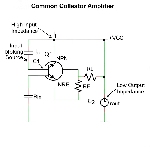
This section delves into the common collector amplifier and its unique characteristics, primarily through numerical examples and design guidelines. The common collector (also known as emitter follower) configuration provides high input impedance and low output impedance, making it particularly useful in applications requiring impedance matching.
Key Parameters:
- Voltage Gain: The voltage gain is expected to be as close to 1 as possible, ensuring minimal signal attenuation.
- Input Impedance: Designed to be very high, allowing the amplifier to work effectively with signal sources.
- Output Impedance: Kept low to maximize power transfer to the load.
- Capacitance and Frequency Response: The impact of load capacitance on the upper cutoff frequency is significant for circuit performance.
Numerical examples provided in this chapter illustrate how to calculate operating points, small signal parameters, and the impact of various resistances and capacitances on the overall circuit behavior. The significance of understanding these parameters is crucial for effective circuit design in real-world applications.
Youtube Videos

Audio Book
Dive deep into the subject with an immersive audiobook experience.
Introduction to the Common Collector Amplifier
Chapter 1 of 7
🔒 Unlock Audio Chapter
Sign up and enroll to access the full audio experience
Chapter Content
So today, we are going to continue the discussion on Common Collector and Common Drain Amplifiers.
Detailed Explanation
In this section, we focus on understanding the common collector amplifier, which is utilized to enhance the input impedance while maintaining a close-to-unity voltage gain. The common collector configuration is also known as an emitter follower.
Examples & Analogies
Think of a common collector amplifier like a gatekeeper at a club. It ensures that only certain guests (signals) can access the main party (output), while allowing the guests to come in without changing their nature (voltage) significantly.
Parameters and Components of the Amplifier
Chapter 2 of 7
🔒 Unlock Audio Chapter
Sign up and enroll to access the full audio experience
Chapter Content
So, we do have the VBB making a bias at the base terminal and then we do have the DC supply of 10 V. So, VBB is given as 6 V. We assume that the thermal equivalent voltage is 26 mV; load capacitance connected at the output node; CL and its value is 100 pF.
Detailed Explanation
The parameters defined here are critical for the operation of the amplifier. The base bias voltage (VBB) sets the initial conditions for the transistor operation, while the DC supply voltage and thermal equivalent voltage affect how the transistor responds to input signals. The load capacitance (CL) plays a role in the frequency response of the amplifier.
Examples & Analogies
Imagine a tank filled with water (the DC supply) where you can control the height with a tap (the base voltage). The load capacitance is like a sponge at the outlet; it can absorb and release water, affecting how quickly the tank can fill or drain.
Defining the Operating Point
Chapter 3 of 7
🔒 Unlock Audio Chapter
Sign up and enroll to access the full audio experience
Chapter Content
If I analyze this circuit and if I consider bias current of 0.5 mA, the collector current is also approximately equal to the emitter current at 0.5 mA.
Detailed Explanation
The operating point of a transistor indicates where it will function optimally. Here, the collector and emitter currents are both around 0.5 mA, allowing for proper conduction in the active region of the transistor. The base voltage and emitter voltage are calculated using the bias conditions established.
Examples & Analogies
Think of the operating point as a sweet spot on a seesaw that allows it to balance evenly. If both sides (the collector and emitter currents) are equal, the seesaw remains stable and efficient.
Small Signal Parameters
Chapter 4 of 7
🔒 Unlock Audio Chapter
Sign up and enroll to access the full audio experience
Chapter Content
We need to find small signal parameters values namely, gm and rπ. For gm, it's the collector current divided by thermal equivalent voltage.
Detailed Explanation
Small signal parameters are essential for determining how the amplifier behaves under small input variations. The transconductance (gm) is calculated as the ratio of the collector current to the thermal voltage, which shows how effectively the transistor can convert changes in input voltage to changes in output current.
Examples & Analogies
Imagine a car's engine. The transconductance is like the car's responsiveness to the gas pedal: how quickly the engine can adjust power output with changes in pedal pressure.
Calculating Voltage Gain
Chapter 5 of 7
🔒 Unlock Audio Chapter
Sign up and enroll to access the full audio experience
Chapter Content
The expression of the voltage gain for this circuit is (gm ro + 1) in the numerator, and in the denominator we do have (gm ro + 1) rπ + ro.
Detailed Explanation
The voltage gain of the common collector amplifier is derived from the relationship between the output and input signals. The gain aims to be as close to unity (1.0) as possible, ensuring minimal attenuation of the input signal. The fine calculations help us determine how much the output signal will mimic the input signal.
Examples & Analogies
This is like a perfectly reflective glass surface where the image (output signal) matches the original picture (input signal) exactly, leading to a clear and unaltered reflection.
Input and Output Impedance
Chapter 6 of 7
🔒 Unlock Audio Chapter
Sign up and enroll to access the full audio experience
Chapter Content
Input resistance looking into this circuit can be approximated as R in = (β + 1) rπ + ro.
Detailed Explanation
The input impedance defines how much the circuit resists incoming signals, while the output impedance indicates how the circuit deals with the load it's driving. Both of these parameters are important for ensuring that the amplifier works efficiently with connected components.
Examples & Analogies
Think of input impedance like a thick wall at the entrance of a venue. Only a few visitors (signals) can approach it without any challenge. On the other hand, output impedance is like the size of the exit door; a larger door allows more guests (current) to leave quickly.
Frequency Response and Cutoff Frequency
Chapter 7 of 7
🔒 Unlock Audio Chapter
Sign up and enroll to access the full audio experience
Chapter Content
The upper cutoff frequency can be calculated as f_upper = 1/(2πRC), where R is the output resistance and C is the load capacitance.
Detailed Explanation
The cutoff frequency gives insight into how the amplifier reacts to different frequencies. It helps determine the bandwidth and frequency response of the amplifier, indicating the range of frequencies the amplifier can handle effectively.
Examples & Analogies
Consider this like tuning a radio; certain frequencies come in clearer than others. The cutoff frequency is akin to finding the best frequency for clear sound quality.
Key Concepts
-
Common Collector Configuration: High input resistance and low output resistance.
-
Voltage Gain: Typically close to 1 for minimal attenuation.
-
Input and Output Impedance: Key parameters affect circuit interfacing.
-
Transconductance Importance: Determines gain and effectiveness of signal transfer.
Examples & Applications
An example of calculating the voltage gain in a common collector amplifier setup involves using the formula A = (gm * Ro) / (1 + gm * Rs) based on defined parameters.
For an amplifier with a bias current of 0.5 mA, determining the emitter voltage requires knowing the base-emitter voltage drop (typically 0.6V).
Memory Aids
Interactive tools to help you remember key concepts
Rhymes
In a collector that's common, resistors do hum, inputs are high, outputs are low; signals flow and never slow.
Stories
Imagine a speaker at a concert, high up in the front where the signals are strong. The speaker (the amplifier) needs to keep up with flows (the high input/output properties) to not disturb the performance.
Memory Tools
To remember the small-signal parameters: 'GROoMs' - Gain, Resistance Output, and small signal M (transconductance).
Acronyms
Use 'GIRL' - Gain Input Resistance Low output for key features of the common collector amplifier.
Flash Cards
Glossary
- Common Collector Amplifier
An amplifier configuration with high input impedance and low output impedance, serving mainly as a buffer.
- Voltage Gain
The ratio of output voltage to input voltage in an amplifier circuit.
- Input Impedance
The impedance seen by the input source of the amplifier, ideally should be high.
- Output Impedance
The impedance looking into the output of the amplifier, ideally should be low.
- Transconductance (gm)
A measure of how effectively an amplifier can control output current relative to the input voltage.
Reference links
Supplementary resources to enhance your learning experience.