
Outline of Today’s Presentation
Enroll to start learning
You’ve not yet enrolled in this course. Please enroll for free to listen to audio lessons, classroom podcasts and take practice test.
Interactive Audio Lesson
Listen to a student-teacher conversation explaining the topic in a relatable way.
Introduction to Amplifiers
🔒 Unlock Audio Lesson
Sign up and enroll to listen to this audio lesson

Today, we're diving deep into common collector and common drain amplifiers. Can anyone tell me why these amplifiers are crucial in circuit design?

I think they are important because they help to increase current while keeping the voltage levels stable.
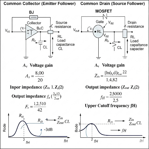
Exactly! Common collector amplifiers, also known as emmitter followers, provide a high input impedance and low output impedance. This is vital for interfacing between different circuit stages. Now, let’s move on to the specific parameters we will discuss today.

What parameters are we looking at?
Great question! We will focus on voltage gain, input-output impedance, and how these are affected by various factors like load resistance and parasitic capacitance.
Understanding Key Metrics
🔒 Unlock Audio Lesson
Sign up and enroll to listen to this audio lesson

Let's discuss voltage gain. Can anyone explain what voltage gain means?

Isn’t it the ratio of output voltage to input voltage?
Correct! In common collector amplifiers, we design for a voltage gain close to 1, which indicates minimal loss. Now, does anyone know why having high input and low output impedance is beneficial?

High input impedance prevents loading issues with previous stages, and low output impedance helps deliver power to the load efficiently!
Spot on! Those characteristics ensure that our amplifier functions effectively in various configurations.
Parasitic Elements and Their Effects
🔒 Unlock Audio Lesson
Sign up and enroll to listen to this audio lesson
Now we need to address parasitics like source resistance and capacitances that affect our amplifier. Why do you think they are critical to consider?
They can change how the circuit behaves and could lead to unexpected losses or changes in performance.
Exactly! They can lower voltage gain or shift cutoff frequencies. This is crucial when designing for specific requirements in real-world applications.
So, managing these parasitics would improve the overall amplifier response?
Right! Effective management leads to better performance metrics that align with design goals.
Numerical Example Walkthrough
🔒 Unlock Audio Lesson
Sign up and enroll to listen to this audio lesson
Let's analyze an example where the DC supply is 10V and the bias voltage is 6V. Can you identify how to start solving for the operating point?
Should we start by calculating the collector and emitter currents based on the bias current?
Exactly! The collector current should approximately equal the emitter current. Once we have that, we can find the operating points for voltage. Let’s proceed step by step together!
I see, we also need to consider voltage drops across resistors when determining the output voltage, right?
Exactly! Those calculations are crucial for ensuring that the transistor stays in the active region.
Introduction & Overview
Read summaries of the section's main ideas at different levels of detail.
Quick Overview
Standard
In this session, we will explore numerical examples and design guidelines related to common collector and common drain amplifiers, utilizing previously discussed knowledge on voltage gain, impedance, and capacitance while accounting for various parasitics.
Detailed
In this section, we will present an outline that emphasizes numerical examples involving common collector and common drain amplifiers. The session will cover essential components such as input-output parameters, the effects of source resistance, load capacitance, and other practical considerations that influence the design of these amplifiers. The key metrics of interest include voltage gain, input and output impedance, and upper cutoff frequency, and we will also derive relevant formulas to encapsulate these relationships clearly. Furthermore, the significance of ensuring the amplifier operates within the active region is highlighted through necessary calculations.
Youtube Videos

Audio Book
Dive deep into the subject with an immersive audiobook experience.
Focus on Numerical Examples
Chapter 1 of 3
🔒 Unlock Audio Chapter
Sign up and enroll to access the full audio experience
Chapter Content
So today, we are going to continue the discussion on Common Collector and Common Drain Amplifiers.
Detailed Explanation
In this presentation, the primary focus will be on numerical examples pertaining to common collector and common drain amplifiers. This means we will be working on practical problems that help us understand how these amplifiers work in real scenarios.
Examples & Analogies
Think of it like learning to ride a bike. While understanding how to balance and pedal is essential, actually getting on the bike and practicing is what truly makes you proficient. Numerical examples act as that practice in the context of electronic circuits.
Review of Previous Knowledge
Chapter 2 of 3
🔒 Unlock Audio Chapter
Sign up and enroll to access the full audio experience
Chapter Content
The knowledge we have gathered in our previous discussion namely, the analysis of voltage gain impedance and capacitance of common collector and common drain circuit for ideal situation as well as considering the different parasitics namely, source resistance, load resistance and collector or drain terminal resistances.
Detailed Explanation
Before diving into new examples, it’s important to review what we've learned previously. We’ve discussed how to analyze voltage gain and impedance for these amplifiers, considering both ideal conditions and real-world factors such as parasitic capacitances and resistances. This foundation is critical as we apply this knowledge in the examples today.
Examples & Analogies
Imagine a chef preparing a complicated dish. Before starting, they must gather and understand their ingredients and tools—just as we must recall our foundational knowledge about amplifiers before tackling new problems.
Structure of Today’s Discussion
Chapter 3 of 3
🔒 Unlock Audio Chapter
Sign up and enroll to access the full audio experience
Chapter Content
What we need to do is to find the operating point of the transistor or the circuit and then small signal parameters values namely, g m and g d of the transistor.
Detailed Explanation
As we proceed through the examples, our goal will be to identify the operating conditions of the transistor, known as the operating point. We’ll also find values for key small signal parameters, specifically transconductance (g m) and output conductance (g d). These parameters are vital for evaluating the performance of the amplifier circuits.
Examples & Analogies
Think of a doctor checking the vital signs of a patient to determine their health condition. Similarly, determining the operating point and small signal parameters gives us insights into how well the transistor operates within the circuit.
Key Concepts
-
Voltage Gain: The ratio of output to input voltage.
-
Impedance: Resistance against AC signals.
-
Parasitics: Unwanted elements that can alter circuit performance.
Examples & Applications
In a common collector configuration with a bias voltage of 6V, calculating the collector current helps establish the operating point.
If the load capacitance is 100 pF, the upper cutoff frequency can be estimated to ensure the amplifier functions effectively.
Memory Aids
Interactive tools to help you remember key concepts
Rhymes
When voltage is stable and currents rise, a common collector is the amplifier prize.
Stories
Imagine a stage where voltage needs to stay the same, while current dancers come and sway smoothly—this is the job of a common collector.
Memory Tools
Use 'VICS' to remember key concepts: Voltage gain, Input impedance, Capacitor effects, Source resistance.
Acronyms
R.I.C.E. to recall
Resistance (input/output)
Impedance
Common collector
and Effective operation.
Flash Cards
Glossary
- Common Collector Amplifier
A type of transistor amplifier that follows the input voltage while providing increased current.
- Voltage Gain
The ratio of output voltage to input voltage in an amplifier.
- Impedance
Resistance of a circuit to the flow of an alternating current, expressed in ohms.
- Parasitic Capacitance
Unintentional capacitances in a circuit that can affect performance.
- Operating Point
The DC voltage and current at which a circuit operates under no signal conditions.
Reference links
Supplementary resources to enhance your learning experience.