
Design Considerations for CMOS Voltage References
Enroll to start learning
You’ve not yet enrolled in this course. Please enroll for free to listen to audio lessons, classroom podcasts and take practice test.
Interactive Audio Lesson
Listen to a student-teacher conversation explaining the topic in a relatable way.
Output Voltage Range
🔒 Unlock Audio Lesson
Sign up and enroll to listen to this audio lesson

Let's start by discussing the output voltage range. Why is it crucial for CMOS voltage references to have a specific output voltage range?

It's important because the voltage needs to meet the requirements of the application, right?
Exactly! A common output is around 1.2 V when using bandgap references. However, the specific output voltage can depend on various design factors, so we have to tailor this based on application needs.

Does the application really translate directly to what voltage we choose?
Definitely. For example, an ADC might require a different voltage than a sensor interface. Remember this: 'V for Voltage, A for Application'. This way, it helps us align voltage selection based on the application needs.

Got it! Why is 1.2 V commonly used?
Great question! It’s often the sweet spot balancing performance and usability in many designs.
To summarize so far, the output voltage range must meet the application's requirements, and common outputs, like 1.2 V, are often influenced by standard practices in circuit design.
Temperature Coefficient
🔒 Unlock Audio Lesson
Sign up and enroll to listen to this audio lesson

Next, let’s talk about the temperature coefficient. What does this term mean in the context of CMOS voltage references?

I think it has to do with how the voltage output changes with temperature.
Correct! Ideally, we want a voltage reference with a zero temperature coefficient. It means the output voltage remains stable regardless of temperature changes. Can anyone think of a way to achieve this?
Using complementary transistors that can balance each other?
Exactly! The idea is to use pairs of transistors or diodes that have opposing temperature coefficients, which helps cancel out the variation. Remember: 'Complementarity Equals Stability'—a helpful mnemonic!
That’s a neat way to remember it!
To summarize, the temperature coefficient is crucial in design, and compensating techniques such as complementary configurations are essential for achieving a stable output voltage.
Power Consumption
🔒 Unlock Audio Lesson
Sign up and enroll to listen to this audio lesson
Let’s shift our focus to power consumption. Why is it particularly important in voltage reference design?
Because many applications are battery-powered, right?
That's right! Low power consumption is a crucial necessity in portable devices. What strategies could we use to reduce power usage in our designs?
We could use low-current transistors?
Very good! Using low-current transistors and lowering bias currents can help achieve this. A useful way to recall this is 'Less Current, More Life'—it highlights how we reduce power while enhancing battery longevity.
That's a smart memory aid!
Summarizing, effective power management is key, particularly in battery-dependent designs, and using strategies like low-current transistors is essential to achieving that.
Load Regulation
🔒 Unlock Audio Lesson
Sign up and enroll to listen to this audio lesson
Now, let’s explore load regulation. Who can explain what this term means?
Is it how well the voltage can maintain stability when the load changes?
Exactly! A good voltage reference should maintain a stable output voltage even when the load current fluctuates. What methods can we use to improve load regulation?
I guess feedback mechanisms and buffering?
Right again! Incorporating feedback loops and buffering stages can enhance load regulation. A helpful way to remember this is 'Feedback for Balance'—signifying the importance of steady voltage amidst changing loads.
That’s a good tip!
In summary, maintaining load regulation is essential for voltage references, and utilizing feedback and buffers is key to achieving stability under varying load conditions.
Noise and Ripple
🔒 Unlock Audio Lesson
Sign up and enroll to listen to this audio lesson
Finally, let's discuss noise and ripple. Why are these factors critical in voltage reference design?
Because noise could affect the accuracy of sensitive systems like ADCs?
Exactly! Low noise levels are significant for stable voltage output, especially in precision applications. What techniques can be used to minimize noise and ripple?
Maybe by using capacitors for filtering?
Correct! Filtering using capacitors is an effective strategy to mitigate unwanted noise. A mnemonic I suggest is 'Capacitance Cleans Output'—easy to recall how filtering helps improve performance.
That’s helpful!
To summarize, minimizing noise and ripple is vital for enhancing the reliability of voltage references, and proper filtering techniques play a crucial role in achieving this.
Introduction & Overview
Read summaries of the section's main ideas at different levels of detail.
Quick Overview
Standard
In this segment, we delve into essential factors influencing the design of CMOS voltage references, including the required output voltage range for the application, the importance of minimizing the temperature coefficient, managing power consumption, maintaining load regulation, and ensuring low noise levels. These considerations significantly impact the performance and reliability of voltage reference circuits.
Detailed
Design Considerations for CMOS Voltage References
In CMOS technology, voltage references are pivotal for various applications, and their effectiveness hinges on several design considerations. This section details crucial parameters that must be managed to optimize voltage reference performance:
1. Output Voltage Range
The output voltage must align with the application's requirements, with a common target of around 1.2 V due to bandgap circuits but adaptable per design specifications.
2. Temperature Coefficient
Minimizing the temperature coefficient is vital for stability; ideally, a voltage reference should maintain a constant output across varying temperatures. Techniques such as using complementary transistors to counteract differing coefficient effects are essential for successful compensation.
3. Power Consumption
Low power use is critical, particularly in battery-operated devices. Employing low-current transistors and minimizing bias currents are effective strategies for creating energy-efficient designs without compromising performance.
4. Load Regulation
Load regulation refers to the voltage output's consistency when load current changes. Implementing feedback mechanisms and buffer stages is crucial for enhancing load regulation, ensuring minimal voltage fluctuation as load conditions vary.
5. Noise and Ripple
For voltage references, low output noise and ripple are necessary for reliable function in sensitive applications like ADCs. Utilizing capacitors and effective filtering techniques can significantly reduce noise and ripple levels, contributing to overall circuit integrity.
In conclusion, these considerations are paramount for designing reliable, accurate, and energy-efficient CMOS voltage references that perform well across varying conditions.
Youtube Videos

Audio Book
Dive deep into the subject with an immersive audiobook experience.
Output Voltage Range
Chapter 1 of 5
🔒 Unlock Audio Chapter
Sign up and enroll to access the full audio experience
Chapter Content
The output voltage of the reference circuit should be within the required range for the application. For example, a common output voltage for CMOS voltage references is 1.2 V (using bandgap reference circuits), but other voltages can be achieved depending on the design.
Detailed Explanation
This chunk discusses the importance of ensuring the output voltage from a CMOS voltage reference circuit matches the application's requirements. For instance, while many circuits, especially those using bandgap references, have a standard output voltage of 1.2 V, it is crucial for designers to adjust this voltage to meet specific needs as different applications might require different reference voltages. The voltage reference must be designed to produce the correct and stable voltage under various operating conditions.
Examples & Analogies
Think of a voltage reference like a water faucet that needs to deliver precise amounts of water for different tasks. If you're filling a glass, you need a steady flow; if you're watering a garden with different plants needing various levels of hydration, you'll need to adjust the flow to meet those specific needs.
Temperature Coefficient
Chapter 2 of 5
🔒 Unlock Audio Chapter
Sign up and enroll to access the full audio experience
Chapter Content
The temperature coefficient of a voltage reference is a key parameter that must be minimized in the design. Ideally, a voltage reference should have a zero temperature coefficient, meaning the output voltage remains constant regardless of temperature changes.
● Temperature Compensation: Using complementary transistors or diodes with opposing temperature coefficients can help achieve temperature compensation.
Detailed Explanation
This chunk highlights the significance of the temperature coefficient in voltage references, which indicates how much the output voltage changes with temperature. A perfect voltage reference would have a temperature coefficient of zero, ensuring that temperature fluctuations do not affect the output voltage. To achieve this, designers often use pairs of complementary transistors or diodes that have opposite responses to temperature changes, effectively cancelling each other out and stabilizing the output voltage.
Examples & Analogies
Imagine two friends who have opposite reactions to seasons. One friend feels energetic in hot weather, while the other feels down. If they work together on a project, their contrasting responses might balance out to maintain a steady productivity level year-round, no matter how hot or cold it gets.
Power Consumption
Chapter 3 of 5
🔒 Unlock Audio Chapter
Sign up and enroll to access the full audio experience
Chapter Content
The power consumption of the voltage reference should be minimized, especially in battery-powered applications. Low-power reference designs are typically required in portable devices.
● Low Power Design: Using low-current transistors and reducing bias currents can help lower power consumption without compromising performance.
Detailed Explanation
This chunk addresses the necessity of minimizing power consumption in voltage reference circuits, particularly in devices that rely on batteries. Since these devices typically operate on limited power supplies, it's crucial to design voltage references that require as little power as possible. Techniques such as utilizing low-current transistors and optimizing bias currents can significantly enhance energy efficiency while keeping the circuit performance intact.
Examples & Analogies
Imagine a smartphone that needs to keep running all day long. If the apps it runs are energy-efficient, the phone will last longer on a single charge. Just like how certain apps can conserve battery, low-power designs in voltage references help keep devices functioning efficiently without draining the battery.
Load Regulation
Chapter 4 of 5
🔒 Unlock Audio Chapter
Sign up and enroll to access the full audio experience
Chapter Content
Load regulation refers to how the output voltage varies when the load current changes. A good voltage reference should maintain a stable output voltage even when the load current fluctuates.
● Feedback and Buffering: Use feedback mechanisms and buffer stages to improve load regulation and minimize voltage fluctuations.
Detailed Explanation
This chunk focuses on load regulation, which measures how stable the output voltage remains when the current drawn by the connected load changes. Effective load regulation is essential to ensure consistent performance in voltage reference circuits. Implementing feedback mechanisms and buffer stages allows for adjustments to be made in real time, preventing significant voltage drops or spikes when the load varies.
Examples & Analogies
Think of load regulation like balancing a tightrope while carrying different weights. If you can adjust your stance and keep your center of gravity steady every time you add or remove weight, you'll maintain your balance. Similarly, good load regulation allows the voltage reference to stay steady, despite changes in the load it must support.
Noise and Ripple
Chapter 5 of 5
🔒 Unlock Audio Chapter
Sign up and enroll to access the full audio experience
Chapter Content
Voltage references should have low noise and low ripple to ensure clean, stable voltage output, especially in sensitive applications like ADCs or precision circuits.
● Filtering: Using capacitors and proper filtering techniques can help reduce noise and ripple in the output.
Detailed Explanation
This chunk emphasizes the importance of having low noise and ripple in voltage references, as these factors can significantly affect the reliability of applications like Analog-to-Digital Converters (ADCs). Noise refers to unwanted variations in voltage, while ripple pertains to fluctuations that occur in electrical signals. To mitigate these issues, designers often employ capacitors and other filtering techniques that help smooth out the output, ensuring it remains stable and precise.
Examples & Analogies
Imagine trying to listen to your favorite music while a group of people talks loudly nearby. The music becomes hard to hear and enjoy due to all that background noise. If you can isolate the sound by using noise-cancelling headphones, you'll hear the music much clearer—just like filtering techniques help ensure a voltage reference produces a clean and stable signal.
Key Concepts
-
Output Voltage Range: Must align with application needs, usually around 1.2 V for many designs.
-
Temperature Coefficient: Ideally kept at zero for stable output across varying temperatures.
-
Power Consumption: Should be minimized, particularly for battery-operated devices.
-
Load Regulation: Maintains stable output voltage despite fluctuations in load current.
-
Noise and Ripple: Must be reduced to ensure reliable outputs in sensitive applications.
Examples & Applications
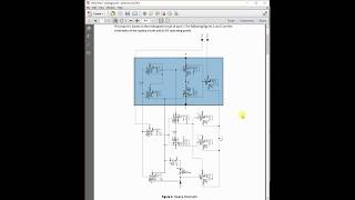
Example of a typical bandgap voltage reference outputting 1.2 V shows how adjusting transistor configurations can stabilize the output.
Using capacitors in feedback mechanisms to reduce ripple in voltage regulation circuits can greatly enhance performance in ADC designs.
Memory Aids
Interactive tools to help you remember key concepts
Rhymes
To keep the voltage just right, during day and night, temperature changes we’ll fight, with complementary light.
Stories
Imagine two friends, one hot and one cold, balancing each other out to keep their temperature stable. This story represents how complementary transistors cancel out different coefficients.
Memory Tools
Remember 'CPRL' for the key design factors: C for Coefficient, P for Power, R for Regulation, L for Load.
Acronyms
NOISE means Need to Optimize and Integrate Silent Energy (to minimize noise in circuits).
Flash Cards
Glossary
- Output Voltage Range
The range of voltages that a voltage reference circuit can provide, which needs to meet application requirements.
- Temperature Coefficient
A parameter indicating how the output voltage of a reference circuit changes with temperature.
- Power Consumption
The amount of power used by a voltage reference circuit, critical in battery-powered applications.
- Load Regulation
The ability of a voltage reference to maintain a stable output voltage when the load current varies.
- Noise and Ripple
Unwanted electrical fluctuations that can affect the stability and accuracy of the voltage output in reference circuits.
Reference links
Supplementary resources to enhance your learning experience.