
Basic CMOS Digital Circuits
Enroll to start learning
You’ve not yet enrolled in this course. Please enroll for free to listen to audio lessons, classroom podcasts and take practice test.
Interactive Audio Lesson
Listen to a student-teacher conversation explaining the topic in a relatable way.
CMOS Logic Gates
🔒 Unlock Audio Lesson
Sign up and enroll to listen to this audio lesson

Today we're going to discuss CMOS logic gates. Can anyone remind me what NMOS and PMOS transistors do?

NMOS transistors conduct when the input is high, right?
Correct! And PMOS transistors conduct when the input is low. This allows us to create different logic operations. Who can tell me the function of the Inverter gate?

It outputs the opposite of the input signal!
Exactly! Now, can someone give me an example of a universal gate?

The NAND gate is a universal gate because you can make any other gate with it!
Great example! Remember, NAND gates are essential because they can be used to replicate any other logic function.
Designing a CMOS Gate
🔒 Unlock Audio Lesson
Sign up and enroll to listen to this audio lesson

Now let's discuss the steps involved in designing a basic CMOS gate. What do you think the first step is?

To determine the logic function?
Yes! After that, we select the number of NMOS and PMOS transistors needed. Why is this important?
It influences the gate's performance, like speed and power!
Well said! Then we connect the transistors to form the complementary network. Can someone tell me how we verify our design afterward?
By creating a truth table?
Correct! It ensures the correct output for our gate. Fantastic job!
Truth Tables
🔒 Unlock Audio Lesson
Sign up and enroll to listen to this audio lesson
Let's dive into truth tables. What is the output of a simple NAND gate if both inputs are high?
The output would be low.
Exactly! And in which cases does the output of a NOR gate turn high?
Only when both inputs are low!
Perfect. Truth tables are powerful tools that help us ensure our design adheres to the expected logical operations.
Complex Gates: XOR and XNOR
🔒 Unlock Audio Lesson
Sign up and enroll to listen to this audio lesson
Now let’s talk about the XOR gate. Can anyone tell me when it outputs high?
It outputs high when one input is high and the other is low!
Correct! And what's the difference with the XNOR gate?
XNOR outputs high when both inputs are the same!
Exactly right! Great work identifying the differences. These gates are integral in various digital applications.
Practical Applications of CMOS Logic Gates
🔒 Unlock Audio Lesson
Sign up and enroll to listen to this audio lesson
Finally, let’s talk about where we find these CMOS gates in real life. Can anyone think of examples?
They are used in microprocessors!
Right! And also in memory storage and signal processing. Can anyone explain why CMOS technology is preferred?
It’s because of low power consumption and high noise immunity!
Excellent job! CMOS technology allows us to design efficient and reliable digital circuits.
Introduction & Overview
Read summaries of the section's main ideas at different levels of detail.
Quick Overview
Standard
In this section, we delve into the design and implementation of basic CMOS digital circuits. It focuses on understanding CMOS logic gates, their configurations, truth tables, and the operational details for Inverters, NAND, NOR, XOR, and XNOR gates, emphasizing on the holistic design procedure and analysis that informs their utility in digital devices.
Detailed
Basic CMOS Digital Circuits
In this section, we explore the essential elements of CMOS digital circuits, specifically the logic gates integral to digital logic design. Transistors (NMOS and PMOS) serve as the building blocks of these circuits, allowing us to construct various logical operations by arranging them into gates such as Inverter, NAND, NOR, XOR, and XNOR.
CMOS Logic Gates Recap
CMOS logic gates exert control over digital signals with two primary types of transistors. The following are fundamental gates:
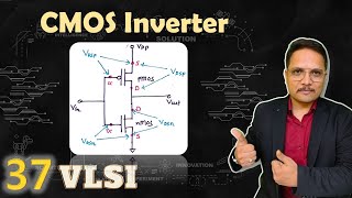
- Inverter: Outputs the opposite of the input signal.
- NAND Gate: Produces a low output when all inputs are high. It is noted for its universality in digital design.
- NOR Gate: Outputs high only when all inputs are low.
- XOR Gate: Outputs high when an odd number of inputs are high.
- XNOR Gate: Outputs high when an even number of inputs are high.
CMOS Logic Gate Design
A structured approach to designing CMOS gates includes:
1. Determine the Logic Function: Clarify the logical operation required.
2. Choose the Number of Transistors: Based on the required function, select NMOS and PMOS counts accordingly.
3. Connect Transistors: Construct the complementary network, ensuring proper flow from input to output.
4. Analyze the Truth Table: Validating the design through truth tables guarantees correct output behavior.
This section not only introduces CMOS technology's foundational concepts but also underlines the essential methodologies employed in designing and analyzing these circuits for real-world applications.
Youtube Videos


Audio Book
Dive deep into the subject with an immersive audiobook experience.
CMOS Logic Gates Recap
Chapter 1 of 2
🔒 Unlock Audio Chapter
Sign up and enroll to access the full audio experience
Chapter Content
As discussed in Chapter 6, CMOS logic gates are the basic building blocks for digital circuits. Each gate performs a specific logical operation and can be implemented using complementary NMOS and PMOS transistors.
● Inverter: The simplest logic gate, which outputs the inverse of the input signal.
● NAND: A universal gate that produces an output that is the inverse of the AND operation.
● NOR: A universal gate that produces an output that is the inverse of the OR operation.
● XOR: Performs the exclusive OR operation, outputting high when exactly one input is high.
● XNOR: The complement of XOR, outputting high when both inputs are the same.
Detailed Explanation
This chunk introduces CMOS logic gates, which are essential components for building digital circuits. Each gate performs basic logical operations, which represent fundamental concepts in digital electronics. For example, an inverter flips the input signal; if you input a 0, you get a 1, and vice versa. NAND and NOR gates are considered universal because you can construct any other logic gate using just these two types, showing their critical role in circuit design. XOR and XNOR gates handle more complex conditions, where the output depends on the specific arrangement of the inputs. Understanding these gates is crucial for anyone studying or working with digital electronics.
Examples & Analogies
Imagine you are in a classroom with a light switch (the inverter). When the switch is off (0), the light is off (0), and when you turn it on (1), the light turns on (1). Now, if we think of NAND as a universal tool, it’s like a Swiss Army knife that can perform multiple functions according to your needs in the classroom. You can use it to cut, twist, or turn things based on your requirements. Thus, these logic gates are like tools that help you manipulate digital information in various ways.
CMOS Logic Gate Design
Chapter 2 of 2
🔒 Unlock Audio Chapter
Sign up and enroll to access the full audio experience
Chapter Content
Each CMOS logic gate is designed by arranging NMOS and PMOS transistors in complementary configurations. Here are some steps for designing a basic CMOS gate:
1. Determine the Logic Function: The first step in designing a logic gate is to determine the desired logical operation (e.g., AND, OR, NOT).
2. Choose the Number of Transistors: Based on the logic function, select the appropriate number of NMOS and PMOS transistors. For example, in a NAND gate, two NMOS transistors are placed in series, while two PMOS transistors are placed in parallel.
3. Connect Transistors: Connect the NMOS and PMOS transistors to form the complementary network. The input(s) control the gate terminals, and the output is taken from the common drain node.
4. Analyze the Truth Table: Verify the output behavior by creating a truth table for the inputs and outputs.
Detailed Explanation
In this section, we learn how to design a CMOS logic gate, which involves using both NMOS and PMOS transistors in a specific arrangement. The design process begins by figuring out what logical function you want the gate to perform. Next, you select how many transistors you need based on the function. For instance, if you're building a NAND gate, you will need two NMOS transistors in series and two PMOS transistors in parallel. You then connect these transistors in such a way that they perform the intended logic function, and finally, you validate the design using a truth table to ensure it behaves correctly with different input combinations.
Examples & Analogies
Think of designing a logic gate like building a simple machine. First, you decide what you want the machine to do (the logic function), like lifting a box. Then, you figure out the parts you need (transistors). For the lifting action, maybe you need two levers (transistors) that work together. Once you've got your parts, you put them together in a way that they can effectively lift the box when you pull a string (the inputs). Finally, you test your machine with different weights (inputs) to ensure it works as expected.
Key Concepts
-
CMOS Gates: Fundamental building blocks of digital circuits.
-
Transistor Types: NMOS and PMOS work together to create CMOS logic.
-
Gate Configurations: Specific arrangements of transistors for each logic function.
-
Truth Tables: Analyze and verify the behaviors of logic gates.
Examples & Applications
Example of an Inverter: If the input is high (1), the output is low (0); vice-versa.
NAND Gate Truth Table: (0,0) -> 1, (0,1) -> 1, (1,0) -> 1, (1,1) -> 0.
Memory Aids
Interactive tools to help you remember key concepts
Rhymes
For a NAND gate to deny, both inputs must be high.
Stories
Imagine two friends (inputs) deciding to go out. If both say 'yes', they can't go (NAND). If one says 'no', they have a party (NOR)!
Memory Tools
Remember: NMOS = Negative (conducts in positive input); PMOS = Positive (conducts in negative input).
Acronyms
NAND = Not AND (Annihilate when both are high).
Flash Cards
Glossary
- CMOS
Complementary Metal-Oxide-Semiconductor; a technology for constructing integrated circuits.
- NMOS
N-type Metal-Oxide-Semiconductor; a type of MOSFET that conducts when the gate voltage is high.
- PMOS
P-type Metal-Oxide-Semiconductor; a type of MOSFET that conducts when the gate voltage is low.
- NAND Gate
A universal gate that outputs low only when all its inputs are high.
- NOR Gate
A universal gate that outputs high only when all its inputs are low.
- XOR Gate
Exclusively OR; it outputs high when an odd number of inputs are high.
- XNOR Gate
The complement of XOR; it outputs high when inputs are the same.
Reference links
Supplementary resources to enhance your learning experience.