
Design and Analysis of CMOS Digital Circuits
Enroll to start learning
You’ve not yet enrolled in this course. Please enroll for free to listen to audio lessons, classroom podcasts and take practice test.
Interactive Audio Lesson
Listen to a student-teacher conversation explaining the topic in a relatable way.
CMOS Inverter Design
🔒 Unlock Audio Lesson
Sign up and enroll to listen to this audio lesson

Today, we will start with the CMOS inverter. Can anyone tell me what this circuit does?

It inverts the input signal, right?
Exactly! The inverter uses a PMOS connected to Vdd and an NMOS to ground. When the input is high, NMOS pulls the output low. Anyone remember the opposite case?

When the input is low, the PMOS conducts and the output is high.
Correct! Let's talk about key parameters. Who can explain what propagation delay is?

It's the time it takes for the input change to affect the output.
Great! Remember, also, we need to consider power consumption, which can be static when the circuit is idle, but also dynamic during switching.

So, the inverter is efficient until it switches?
Precisely! To summarize, the CMOS inverter consists of PMOS and NMOS transistors, is crucial in logic design, and its performance depends heavily on sizing and delay parameters.
CMOS NAND Gate Design
🔒 Unlock Audio Lesson
Sign up and enroll to listen to this audio lesson

Next, let’s move on to the CMOS NAND gate. Can someone explain its general operation?
The output is low only if both inputs are high?
Exactly! This is due to the series connection of NMOS and parallel for PMOS. Who wants to summarize the truth table?
It’s 1, 1, 0 when both inputs are high, and 1 in all other cases.
Perfect! Why do we say NAND gates are universal?
Because we can create any logic gate from NAND gates!
Exactly! The NAND gate's utility in digital circuits cannot be overstated. Let’s summarize the key points and the truth table again.
CMOS NOR Gate Design
🔒 Unlock Audio Lesson
Sign up and enroll to listen to this audio lesson
Now, let’s discuss the CMOS NOR gate. Who can tell me its output condition?
The output is high only when both inputs are low!
Correct! And how is this configured using transistors?
Two NMOS in parallel and two PMOS in series.
Exactly right! Can anyone help recall the truth table?
It goes: 1, 0, 0, 0 for inputs 0, 0; 0, 1; 1, 0; and 1, 1.
Excellent! This familiarity with basic configuration aids in understanding complex circuits. Who remembers a practical application for NOR gates?
They are often used in alarm systems and data latching circuits.
Great example! Let’s wrap up the NOR gate design and its applications.
CMOS XOR and XNOR Gates
🔒 Unlock Audio Lesson
Sign up and enroll to listen to this audio lesson
Let’s discuss the XOR gate next. What makes it different from other gates?
It outputs high only when one input is high.
Correct! How do we design it using other gates?
By combining NAND and NOR gates.
Right! The truth table shows it goes: high when inputs differ. Now, what about the XNOR gate?
It's the complement of the XOR; it outputs high when inputs are the same.
Exactly! The importance of these gates is immense in digital circuit design. Let’s summarize their functions again.
Introduction & Overview
Read summaries of the section's main ideas at different levels of detail.
Quick Overview
Standard
In this section, we delve into the design principles behind fundamental CMOS digital circuits, including the CMOS inverter, NAND gate, NOR gate, XOR gate, and XNOR gate. Each component's operation, truth tables, and critical parameters such as propagation delay and power consumption are examined, providing a comprehensive overview of CMOS digital circuit design.
Detailed
Design and Analysis of CMOS Digital Circuits
In this section, we explore the specifics of designing and analyzing various CMOS digital circuits. The fundamental building blocks of these circuits include:
7.3.1 CMOS Inverter Design
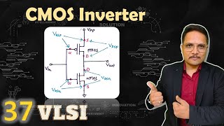
The CMOS inverter consists of a PMOS transistor linked to Vdd (the supply voltage) and an NMOS transistor connected to ground. The basic operation is:
- When the input signal is high (1), NMOS conducts, bringing output low (0).
- Conversely, when the input is low (0), PMOS conducts, bringing output high (1).
Key Parameters:
- Transistor Sizing: The width-to-length ratio (W/L) is vital for drive current and switching speed.
- Propagation Delay: The delay time for the output to respond to input changes.
- Power Consumption: Characterized by high efficiency in static power but also dynamic power during transitions.
7.3.2 CMOS NAND Gate Design
The CMOS NAND gate features two NMOS transistors in series and two PMOS in parallel. Its operation is:
- Output (Vout) is low (0) when both inputs are high (1); otherwise, it's high (1).
Truth Table:
- Inputs (A, B):
- 0, 0 → 1
- 0, 1 → 1
- 1, 0 → 1
- 1, 1 → 0
7.3.3 CMOS NOR Gate Design
The CMOS NOR gate has two NMOS in parallel and two PMOS in series, operating as follows:
- Output is high (1) only when both inputs are low (0).
Truth Table:
- Inputs (A, B):
- 0, 0 → 1
- 0, 1 → 0
- 1, 0 → 0
- 1, 1 → 0
7.3.4 CMOS XOR Gate Design
The CMOS XOR gate is more complex, derived from combinations of NAND and NOR gates:
- Outputs high (1) when exactly one input is high (1).
Truth Table:
- Inputs (A, B):
- 0, 0 → 0
- 0, 1 → 1
- 1, 0 → 1
- 1, 1 → 0
7.3.5 CMOS XNOR Gate Design
The CMOS XNOR gate complements the XOR, providing high output when inputs are identical:
- Outputs high (1) when both inputs match.
Truth Table:
- Inputs (A, B):
- 0, 0 → 1
- 0, 1 → 0
- 1, 0 → 0
- 1, 1 → 1
Understanding these gates' designs enhances a student's grasp of integrated circuit behavior and is crucial for effective digital design.
Youtube Videos


Audio Book
Dive deep into the subject with an immersive audiobook experience.
CMOS Inverter Design
Chapter 1 of 6
🔒 Unlock Audio Chapter
Sign up and enroll to access the full audio experience
Chapter Content
The CMOS inverter is the simplest CMOS logic gate, comprising a PMOS transistor connected to Vdd and an NMOS transistor connected to ground. The input signal is applied to the gates of both transistors, and the output is taken from the common drain node.
Detailed Explanation
A CMOS inverter is a specific type of logic gate that essentially flips the input signal. When you apply a high voltage (represented as 1), the NMOS transistor kicks in and pulls the output down to ground (0). Conversely, when the input is low (0), the PMOS transistor activates, pulling the output high (1). This simple mechanism allows for efficient switching between states.
Examples & Analogies
Think of the CMOS inverter like a light switch in your house. When you flip the switch up (input high), the light (output) is off (0). When you flip the switch down (input low), the light turns on (1). The way the inverter works is analogous to how the switch controls the flow of electricity, turning the output on and off based on the input.
Key Parameters of CMOS Inverters
Chapter 2 of 6
🔒 Unlock Audio Chapter
Sign up and enroll to access the full audio experience
Chapter Content
● Operation:
○ When the input is high (1), the NMOS transistor conducts, pulling the output low (0).
○ When the input is low (0), the PMOS transistor conducts, pulling the output high (1).
● Key Parameters:
○ Transistor Sizing: The width-to-length ratio of the transistors determines the current drive and switching speed.
○ Propagation Delay: The time it takes for the input change to propagate through the inverter and affect the output.
○ Power Consumption: CMOS inverters are highly efficient in terms of static power consumption but can consume dynamic power during switching.
Detailed Explanation
Understanding the operation of the inverter is crucial. The width-to-length ratio of the transistors is significant because it affects how much current they can drive and how quickly they can switch between states. Propagation delay is important as it indicates how fast the inverter can respond to a change in input. Lastly, power consumption tells us how efficiently the inverter operates; ideally, we want to minimize both static (when inactive) and dynamic (when switching) power consumption.
Examples & Analogies
Imagine if your light switch took a long time to respond when you flipping it! That would be similar to a high propagation delay in an inverter. The switch not only needs to respond quickly but also should consume minimal power when not in use. An efficient inverter acts like a well-designed switch that only uses energy when it’s actively turning the light on or off.
CMOS NAND Gate Design
Chapter 3 of 6
🔒 Unlock Audio Chapter
Sign up and enroll to access the full audio experience
Chapter Content
The CMOS NAND gate consists of two NMOS transistors connected in series and two PMOS transistors connected in parallel. The input signal is applied to the gates of both transistors, and the output is taken from the common drain node.
Detailed Explanation
A CMOS NAND gate operates by allowing the output to be low (0) only when both inputs are high (1). This configuration means if either or both inputs are low, the output will be high (1). The NMOS transistors are in series so that they both must conduct for the output to go low, while the PMOS transistors are in parallel, allowing just one to conduct and pull the output high when not all inputs are high.
Examples & Analogies
Think of a gate that only opens if two keys are used at once - both keys represent input signals. If both inputs (keys) are not pressed (high), the gate stays open (output high). This behavior mimics the NAND gate's function, where the output is open unless both conditions are met!
CMOS NOR Gate Design
Chapter 4 of 6
🔒 Unlock Audio Chapter
Sign up and enroll to access the full audio experience
Chapter Content
The CMOS NOR gate consists of two NMOS transistors connected in parallel and two PMOS transistors connected in series.
Detailed Explanation
For a CMOS NOR gate, the output will only be high (1) if both inputs are low (0). If either input is high (1), the output will drop to low (0). The configuration of the NMOS transistors in parallel means that if either one conducts, the output cannot be high. In contrast, since PMOS transistors are in series, both must be off (non-conducting) for the output to be pulled high.
Examples & Analogies
Imagine a door lock that only opens if both keys are not in the lock. If even one key is in (input high), you cannot turn the handle (output is low). This setup illustrates how a NOR gate functions.
CMOS XOR Gate Design
Chapter 5 of 6
🔒 Unlock Audio Chapter
Sign up and enroll to access the full audio experience
Chapter Content
The CMOS XOR gate is more complex than basic gates like NAND and NOR. It can be designed using a combination of NAND and NOR gates. The XOR gate outputs high (1) when exactly one input is high; otherwise, the output is low (0).
Detailed Explanation
The XOR gate's operation hinges on having one, and only one, of its inputs high (1). This means that the output will switch to high (1) if either input A is high while input B is low, or input A is low while input B is high. If both inputs are the same (both high or both low), the output will be low (0). Designing this gate usually requires combining NAND and NOR configurations to achieve the desired logic.
Examples & Analogies
Imagine a party where there are two lights, but you want the main light only to turn on if exactly one of your two friends turns on their respective light. If both friends are off or both are on, the main light stays off. This unique condition reflects how the XOR gate behaves.
CMOS XNOR Gate Design
Chapter 6 of 6
🔒 Unlock Audio Chapter
Sign up and enroll to access the full audio experience
Chapter Content
The CMOS XNOR gate is the complement of the XOR gate. It outputs high (1) when both inputs are the same (either both high or both low).
Detailed Explanation
An XNOR gate turns the traditional XOR operation inside out. Here, the output becomes high (1) only when both inputs match—either both are low (0) or both are high (1). This involves similarly complex arrangements of transistors to negate the XOR behavior seamlessly. The design fundamentally uses the same logic as the XOR but reverses the output requirement.
Examples & Analogies
Picture a situation where you’re checking the dress code at a party. If both friends wear the same color (either both in blue or both in red), that’s acceptable (output high). If one wears blue and the other red, it’s a mismatch (output low). This reflect the behavior of the XNOR gate and how it determines the output based on matching conditions.
Key Concepts
-
CMOS Inverter: The basic building block that inverts input signals.
-
NAND Gate: Outputs low only when all inputs are high, enabling versatility.
-
NOR Gate: Outputs high only when inputs are all low.
-
XOR Gate: High output when one input is true, used for parity checks.
-
XNOR Gate: Outputs high when inputs match, used in error detection.
Examples & Applications
An example of a CMOS inverter in action is in a simple logic circuit where the inverter is used to invert a control signal.
In digital computing, NAND gates can be used to construct memory cells or complex logic functions for processors.
Memory Aids
Interactive tools to help you remember key concepts
Rhymes
IN-verters flip your fate, lend a hand, they don’t wait! High goes down and low goes up, inverted signals fill your cup!
Stories
Imagine building a bridge: each transistor connects with one pulling the car over smoothly, while another pushes back when too heavy. One side wanes and the other flourishes, just like NAND and NOR gates.
Memory Tools
NAND = Not AND (output only low when both inputs are high) so remember: Nearly Always Not Down!
Acronyms
XOR = eXclusive OR, so remember
One should be a lone ranger to keep peace in the XOR land!
Flash Cards
Glossary
- CMOS Inverter
A CMOS logic gate that outputs the opposite of the input signal.
- NAND Gate
A universal logic gate that produces a low output only when all inputs are high.
- NOR Gate
A logic gate that outputs high only when all inputs are low.
- XOR Gate
A digital logic gate that outputs high when exactly one input is true.
- XNOR Gate
A logic gate that outputs high when both inputs are equal.
- Propagation Delay
The time taken for an input change to affect the output.
- Power Consumption
The amount of power used by the circuit during operation.
Reference links
Supplementary resources to enhance your learning experience.