
CMOS Inverter Design
Enroll to start learning
You’ve not yet enrolled in this course. Please enroll for free to listen to audio lessons, classroom podcasts and take practice test.
Interactive Audio Lesson
Listen to a student-teacher conversation explaining the topic in a relatable way.
Introduction to CMOS Inverter
🔒 Unlock Audio Lesson
Sign up and enroll to listen to this audio lesson

Today, we'll discuss the CMOS inverter, which is the simplest form of a logic gate. It's made of one PMOS and one NMOS transistor. Can anyone tell me what happens when we apply a high input?

When the input is high, the NMOS conducts, right?
Exactly! And what does that mean for the output?

It means the output is pulled low.
Correct! Let's remember this as 'HI = LO' for high input leads to low output. Now, what happens when the input is low?

The PMOS conducts, pulling the output high.
Wonderful! So we can remember 'LO = HI' too. Are there any questions so far?
Key Parameters of CMOS Inverter
🔒 Unlock Audio Lesson
Sign up and enroll to listen to this audio lesson

Now let's dive into some key parameters that affect the performance of the CMOS inverter. What do you think influences the switching speed?

Maybe the size of the transistors?
Good point! The width-to-length ratio of the transistors is critical. Larger ratios can improve current drive and speed. Do you remember why propagation delay is significant?
It indicates how quickly the inverter reacts to input changes!
Exactly! Longer delays slow down the overall circuit. Now, what can you tell me about power consumption?
Is it true that CMOS inverters use little power when not switching?
That's correct! They're efficient, but dynamic power comes into play during switching. Great discussion! Let's recap: transistor sizing impacts speed, propagation delay indicates response time, and static vs. dynamic power consumption is crucial for efficiency.
Practical Applications of CMOS Inverters
🔒 Unlock Audio Lesson
Sign up and enroll to listen to this audio lesson
CMOS inverters are used in many applications. Can anyone name a device that relies on them?
Microprocessors use CMOS technology!
Right! They're essential in processors, but also in memory devices. Why do you think low power consumption is beneficial in these applications?
It helps extend battery life in portable devices!
Exactly! Less power also means less heat generation, which is crucial for reliability. This understanding of CMOS inverters sets the stage for exploring other gates. Any lingering questions before we move on?
Introduction & Overview
Read summaries of the section's main ideas at different levels of detail.
Quick Overview
Standard
This section focuses on the design and operational principles of the CMOS inverter, a crucial element in digital circuits. It discusses how the inverter utilizes a PMOS and NMOS transistor to implement logical negation, alongside important parameters such as propagation delay and power consumption.
Detailed
Detailed Summary of CMOS Inverter Design
The CMOS inverter is the fundamental building block of CMOS digital circuits, consisting of a PMOS and an NMOS transistor connected in a complementary configuration. The key operational principle is its ability to output the inverse of the input signal: when the input is high (1), the NMOS conducts, and the output is low (0); conversely, when the input is low (0), the PMOS conducts, pulling the output high (1). This behavior is essential for performing logic operations in digital electronics. The design parameters of the CMOS inverter include:
- Transistor Sizing: The width-to-length ratio of the transistors is critical for determining their current drive capability and switching speed.
- Propagation Delay: This is the time required for an input change to propagate through the inverter and affect the output.
- Power Consumption: CMOS inverters are efficient concerning static power consumption when idle, though they can exhibit dynamic power consumption during operation.
Understanding the design aspects of the CMOS inverter is pivotal as it lays the foundation for more complex logic gates and is a vital component in various digital applications.
Youtube Videos


Audio Book
Dive deep into the subject with an immersive audiobook experience.
Understanding the CMOS Inverter
Chapter 1 of 3
🔒 Unlock Audio Chapter
Sign up and enroll to access the full audio experience
Chapter Content
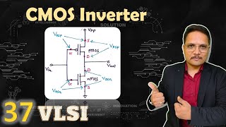
The CMOS inverter is the simplest CMOS logic gate, comprising a PMOS transistor connected to Vdd and an NMOS transistor connected to ground. The input signal is applied to the gates of both transistors, and the output is taken from the common drain node.
Detailed Explanation
A CMOS inverter consists of two types of transistors: PMOS and NMOS. The PMOS transistor is connected to the positive supply voltage (Vdd), and the NMOS is connected to the ground. The input of the inverter controls both transistors. When the input is energized (high), the NMOS turns on, allowing current to flow to ground, thus pulling the output low (0). When the input is de-energized (low), the PMOS turns on instead, driving the output high (1). This inherent output inversion is what makes it a fundamental digital component used in various applications.
Examples & Analogies
Think of the CMOS inverter like a light switch. When you turn the switch on (input high), the light goes off (output low). When you turn the switch off (input low), the light turns on (output high). This simple toggle behavior mimics the functioning of binary logic in digital circuits.
Operation of the CMOS Inverter
Chapter 2 of 3
🔒 Unlock Audio Chapter
Sign up and enroll to access the full audio experience
Chapter Content
● Operation:
○ When the input is high (1), the NMOS transistor conducts, pulling the output low (0).
○ When the input is low (0), the PMOS transistor conducts, pulling the output high (1).
Detailed Explanation
The operation of the CMOS inverter is quite straightforward. When you apply a high voltage (1) to the input, the NMOS transistor is activated. This means it allows electricity to flow from the output to the ground, resulting in the output being pulled down to low (0). Conversely, when the input is low (0), the NMOS turns off, and the PMOS turns on instead, allowing the output to connect to the positive voltage. Thus, the output switches high (1). This interplay between NMOS and PMOS ensures that the inverter effectively reverses the input signal.
Examples & Analogies
Imagine a water gate system. When you turn on the supply of water (high input), water drains through an outlet (output low). However, when you close the water supply (low input), the outlet gets blocked, and the reservoir fills up (output high). This analogy helps us see how the inverter works in managing the flow of power instead of water.
Key Parameters of CMOS Inverter
Chapter 3 of 3
🔒 Unlock Audio Chapter
Sign up and enroll to access the full audio experience
Chapter Content
● Key Parameters:
○ Transistor Sizing: The width-to-length ratio of the transistors determines the current drive and switching speed.
○ Propagation Delay: The time it takes for the input change to propagate through the inverter and affect the output.
○ Power Consumption: CMOS inverters are highly efficient in terms of static power consumption but can consume dynamic power during switching.
Detailed Explanation
The performance of a CMOS inverter hinges on several key parameters. Firstly, transistor sizing — defined by the width-to-length ratio — affects how much current the inverter can drive and how quickly it can switch states. A larger ratio allows more current and faster switching but takes more space on a chip. Secondly, propagation delay is crucial; it measures how long it takes for a change at the input to reflect at the output. This is important for determining the overall speed of the circuit. Lastly, power consumption is another critical factor; while static power is low when not switching, dynamic power use increases during transitions, which must be managed for energy efficiency.
Examples & Analogies
Consider the parameters of a car. The size of the engine (transistor sizing) affects how fast the car can go (switching speed). The time it takes to accelerate to speed (propagation delay) determines how quickly you can be on your way. Additionally, how much fuel (power consumption) you use determines how efficiently you can travel. Just like tuning a car for performance and efficiency, these parameters help optimize the inverter's functionality.
Key Concepts
-
CMOS Inverter: The primary building block of digital circuits that inverts the input signal.
-
Transistor Sizing: Affects the inverter's performance regarding speed and current handling.
-
Propagation Delay: Important for understanding how quickly the inverter responds to input changes.
-
Power Consumption: Critical for efficiency, especially in battery-powered devices.
Examples & Applications
In digital circuits, a CMOS inverter is utilized to form more complex gates, such as NAND and NOR, by arranging multiple inverter configurations.
CMOS inverters are extensively used in microprocessors for their low static power consumption and fast switching capabilities.
Memory Aids
Interactive tools to help you remember key concepts
Rhymes
When the input is high, the output is low; the CMOS inverter steals the show!
Stories
Once upon a time in a digital land, a clever inverter turned signals as planned. When input was high, it whispered 'Hello!' And when the input was low, a high output would glow.
Memory Tools
Use 'HI-LO' to remember that high input yields low output and vice versa for the CMOS inverter.
Acronyms
Remember 'P.T.P.' - Propagation time, Transistor sizing, and Power consumption as key concepts of the CMOS inverter.
Flash Cards
Glossary
- CMOS Inverter
A basic CMOS logic gate that outputs the inverse of the input signal, comprised of a PMOS and NMOS transistor.
- Propagation Delay
The time it takes for an input change to propagate through the circuit and manifest at the output.
- Power Consumption
The total amount of power used by the circuit during its operation, differentiated into static and dynamic consumption.
- Transistor Sizing
The ratio of the width to length of a transistor which affects its current capacity and switching speed.
Reference links
Supplementary resources to enhance your learning experience.