
Flip-Chip Technology
Interactive Audio Lesson
Listen to a student-teacher conversation explaining the topic in a relatable way.
Introduction to Flip-Chip Technology
🔒 Unlock Audio Lesson
Sign up and enroll to listen to this audio lesson

Today, we will dive into flip-chip technology, a fascinating method of semiconductor interconnection. Can anyone tell me what interconnection technology refers to?

Is it how we connect different parts of a semiconductor together?
Exactly! Interconnection technology determines how electrical connections are made. Flip-chip technology specifically involves flipping the IC die and using solder bumps for connections. What do you think are the advantages of this approach?

I think it might allow for more compact designs?
Right! Higher interconnection density is one of its biggest advantages. Remember, we can call that HDI, which stands for High-Density Interconnections. Now, does anyone know about its applications?

It’s used in processors, right?
Yes! It’s commonly used in high-performance processors and graphics cards. Let’s summarize that flip-chip technology provides enhanced performance but at a higher cost and complexity.
Bonding Process of Flip-Chip Technology
🔒 Unlock Audio Lesson
Sign up and enroll to listen to this audio lesson

Now, let’s dive into the bonding process involved in flip-chip technology. What do you think happens when we flip the IC?

We need to make sure the solder bumps align with the PCB, right?
Exactly! The IC must be accurately aligned before the solder bumps are reflowed. This is critical to ensuring strong electrical connections. Why might precise alignment be challenging?
Because if they're not aligned, it might not connect properly.
Correct! A misalignment can lead to poor performance. This is something to always consider when using flip-chip technology. In summary, the bonding process is vital for reliable interconnections.
Advantages and Disadvantages of Flip-Chip
🔒 Unlock Audio Lesson
Sign up and enroll to listen to this audio lesson
Let's discuss the advantages and disadvantages of using flip-chip technology. Who can summarize one advantage?
It provides better thermal performance due to shorter interconnects.
Great! Better thermal performance is a key benefit. Now, can anyone think of a disadvantage?
It seems more complex and could be harder to repair.
Exactly! The complexity can make assembly and rework more challenging. So we’ll remember that while flip-chip offers innovative solutions, it comes with its own set of challenges.
Introduction & Overview
Read summaries of the section's main ideas at different levels of detail.
Quick Overview
Standard
This section discusses flip-chip technology as an advanced interconnection method in semiconductor packaging, highlighting its bonding process, applications, and the advantages and disadvantages that come with it compared to traditional techniques like wire bonding.
Detailed
Flip-Chip Technology
Flip-chip technology is a contemporary interconnection method that plays a critical role in modern semiconductor packaging. In this technique, the integrated circuit (IC) die is flipped upside down, allowing for electrical connections to be made via solder bumps that are directly affixed to the substrate or printed circuit board (PCB). This process not only optimizes space but also significantly enhances the density of interconnections, which is paramount for high-performance applications.
Key Components of Flip-Chip Technology
- Bonding Process: The bonding process involves aligning the flipped IC with the substrate or PCB, where solder bumps are heated to create permanent electrical connections. This method enables a more compact design, incorporating high-density interconnections and minimizing the distance between the chip and external circuits, which is essential for improved performance.
- Applications: Flip-chip technology finds extensive application in modern electronics, particularly within high-performance processors, graphics cards, memory modules, and system-in-package (SiP) solutions.
- Advantages: This technology offers several benefits, including higher interconnect density, superior thermal performance, and improved signal integrity due to reduced inductance.
- Disadvantages: However, the complexities and costs associated with flip-chip assembly present challenges, such as difficult rework processes and the intricacies of aligning components during assembly.
Significance in Semiconductor Manufacturing
As the electronics market progresses towards more compact, efficient solutions, the role of flip-chip technology is expected to become increasingly significant, particularly in fields demanding high performance and reliability.
Youtube Videos

Audio Book
Dive deep into the subject with an immersive audiobook experience.
Bonding Process
Chapter 1 of 4
🔒 Unlock Audio Chapter
Sign up and enroll to access the full audio experience
Chapter Content
The IC is flipped and aligned with the substrate or PCB, and then solder bumps are reflowed to establish electrical connections. Flip-chip bonding enables high-density interconnections and reduces the distance between the chip and the external circuit, improving performance.
Detailed Explanation
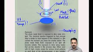
In the flip-chip bonding process, the integrated circuit (IC) is turned upside down so that its active surface faces the substrate or printed circuit board (PCB). Precise alignment is crucial to ensure that the solder bumps, which are small dots of solder material, make contact with corresponding pads on the substrate. Once aligned, the solder bumps undergo a reflow process, where they are heated until they melt and create a solid electrical connection as they cool. This method allows for a compact design and enhances the overall performance by minimizing the distance that electrical signals must travel.
Examples & Analogies
Think of it like assembling a jigsaw puzzle. You have to flip a piece over, align it carefully with the fitting part of the puzzle board, and then press down to secure it. Just like the pieces must fit perfectly to create a complete picture, the IC and substrate must align well for efficient electrical connections.
Applications
Chapter 2 of 4
🔒 Unlock Audio Chapter
Sign up and enroll to access the full audio experience
Chapter Content
Flip-chip technology is widely used in high-performance processors, graphics cards, memory modules, and system-in-package (SiP) applications.
Detailed Explanation
Flip-chip technology is particularly advantageous for various high-performance applications due to its capability to facilitate high-density interconnections. This means it can connect a large number of signals in a compact area, making it perfect for processors that require immense computational power. Graphics cards also benefit from this technology as they need to process large amounts of data quickly. Additionally, memory modules that demand fast and reliable data access utilize flip-chip bonding to ensure optimal performance.
Examples & Analogies
Imagine a busy highway that needs to accommodate a high volume of cars. If we combine several lanes into fewer but more efficient entrances and exits (like high-density connections), we can reduce congestion and improve traffic flow. Flip-chip technology works similarly by streamlining connections in a compact space, enhancing the overall speed and efficiency of electronic devices.
Advantages
Chapter 3 of 4
🔒 Unlock Audio Chapter
Sign up and enroll to access the full audio experience
Chapter Content
High-density interconnections and smaller form factors. Better thermal performance due to shorter interconnects and direct thermal pathways. Reduced inductance and improved signal integrity.
Detailed Explanation
The advantages of flip-chip technology are significant. First, it allows for high-density interconnections, meaning that more connections can fit into a smaller area. This makes it ideal for compact electronic devices. Secondly, because the connections are shorter and more direct, heat can dissipate more efficiently, improving the thermal performance of the overall device. Additionally, shorter interconnects lead to reduced inductance, which is beneficial for signal integrity, especially in high-speed applications. This leads to clearer signals with less interference.
Examples & Analogies
Consider how a direct flight from one city to another is faster and more efficient than a flight with multiple layovers. Similarly, the short and direct connections in flip-chip technology allow electrical signals to travel faster and with fewer interruptions, improving the overall performance of a device.
Disadvantages
Chapter 4 of 4
🔒 Unlock Audio Chapter
Sign up and enroll to access the full audio experience
Chapter Content
More expensive and complex assembly process compared to wire bonding. Difficult rework due to the flip-chip nature of the assembly.
Detailed Explanation
While flip-chip technology offers many benefits, it also comes with disadvantages. The assembly process is often more complex and costly than traditional methods like wire bonding. This complexity arises from the need for precise alignment and specialized equipment for solder bump formation and reflow. Moreover, if a flip-chip assembly needs to be repaired, it is more challenging due to the nature of how the IC is mounted. Unlike wire-bonded devices, which can be reworked by accessing the wires, flip-chip devices require careful handling to avoid damaging the solder joints.
Examples & Analogies
Think of flip-chip assembly like building a complex Lego structure with many intricate connections. If a piece needs to be replaced, it can require disassembling several parts to access the one that’s faulty. This is much more complicated than just finding a simple piece on a flat Lego surface that can be easily swapped out, highlighting the difficulties in repairing a flip-chip assembly.
Key Concepts
-
Bonding Process: The steps involved in making connections using solder bumps in flip-chip technology.
-
Applications: The various electronics that utilize flip-chip technology, including processors and graphics cards.
-
Advantages: Key benefits such as improved thermal performance and higher interconnect density.
-
Disadvantages: Challenges including cost and complexity in assembly and rework.
Examples & Applications
High-performance graphics processors often utilize flip-chip technology for higher efficiency.
Memory module designs frequently adopt flip-chip approaches to minimize space while maximizing performance.
Memory Aids
Interactive tools to help you remember key concepts
Rhymes
Flip-chip, flip-chip, solder in a zip, high density connections, let your performance rip!
Stories
Imagine a race car that switched to hover technology; it sped through turns representing how flip-chip enhances signal performance by reducing distance.
Memory Tools
Remember ‘HARD’ for flip-chip: High density, Alignment crucial, Reliable connections, Difficult rework.
Acronyms
DART - Density, Assembly complexity, Reliability, Thermal performance.
Flash Cards
Glossary
- FlipChip Technology
An advanced interconnection method that involves flipping the IC die upside down to connect directly to the substrate via solder bumps.
- Solder Bumps
Small mounds of solder that are used for electrical interconnections in flip-chip bonding.
- HighDensity Interconnections (HDI)
Refers to the high density of connections achievable by flip-chip technology.
- Bonding Process
The method used to establish electrical connections between the IC and substrate, which in flip-chip involves alignment and solder reflow.
- Printed Circuit Board (PCB)
A board used for electrically connecting and mechanically supporting electronic components.
Reference links
Supplementary resources to enhance your learning experience.