
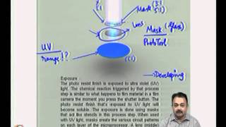
Interconnection Techniques
Interactive Audio Lesson
Listen to a student-teacher conversation explaining the topic in a relatable way.
Introduction to Interconnection Techniques
🔒 Unlock Audio Lesson
Sign up and enroll to listen to this audio lesson

Today, we will learn about the interconnection techniques used in semiconductor packaging. Can anyone tell me why interconnection techniques are important?

They connect the IC to the circuitry on the PCB.
Exactly! They establish the necessary electrical connections. There are three main techniques we will focus on today: wire bonding, flip-chip technology, and solder bump technology.

What’s the difference between these techniques?
Good question! Each technique has unique applications and advantages. We will explore each one in detail.
Wire Bonding
🔒 Unlock Audio Lesson
Sign up and enroll to listen to this audio lesson

Let's start with wire bonding. This is the most common interconnection method. Can someone explain how it works?

I think it uses fine wires to connect the IC to the PCB?
Yes! The process involves creating ball and wedge bonds. Wire bonding is very cost-effective, especially for high-volume production.

What are some disadvantages?
Wire bonding can struggle with high-frequency applications due to longer wires creating inductance issues and it is also susceptible to mechanical stress. Remember: 'Wire bonding = cost-efficient but limited high-speed performance.'
Flip-Chip Technology
🔒 Unlock Audio Lesson
Sign up and enroll to listen to this audio lesson
Next, we have flip-chip technology. Does anyone know how this differs from wire bonding?
Is it where the IC is flipped upside down?
Exactly! It uses solder bumps to connect directly to the PCB. This allows for high-density connections, which is essential in modern devices.
What about the drawbacks?
It is more complex and expensive compared to wire bonding, plus rework can be challenging because of the assembly's nature. To remember this, think 'Flip-chip = high performance but pricey.'
Solder Bump Technology
🔒 Unlock Audio Lesson
Sign up and enroll to listen to this audio lesson
Lastly, let’s delve into solder bump technology. What makes it significant?
It helps create stronger connections, right?
Yes! Solder bumps improve electrical and thermal performance and are perfect for compact designs. But they do require precision and cleanliness.
So, it sounds like there are trade-offs?
Absolutely! Each technique offers a balance of performance, cost, and application suitability. Remember: 'Solder bumps = better performance, more complexity!'
Summary of Techniques
🔒 Unlock Audio Lesson
Sign up and enroll to listen to this audio lesson
To summarize, we learned about three interconnection techniques: wire bonding, flip-chip, and solder bump technology. Who can highlight one key point from each?
Wire bonding is cost-effective!
Flip-chip offers high-density connections!
Solder bump technology gives improved electrical performance!
Fantastic! Remember these key points as they encapsulate the strengths and weaknesses of each technique. Forming connections in semiconductor packaging is both an art and a science.
Introduction & Overview
Read summaries of the section's main ideas at different levels of detail.
Quick Overview
Standard
Interconnection techniques are essential for creating electrical connections between integrated circuits (ICs) and printed circuit boards (PCBs). This section covers three primary interconnection methods: wire bonding, flip-chip technology, and solder bump technology, detailing their processes, applications, advantages, and disadvantages.
Detailed
Interconnection Techniques
Interconnection techniques are critical for establishing electrical connections between integrated circuits (ICs) and the external circuits on printed circuit boards (PCBs). The choice of technique depends on various factors, including cost, performance requirements, and package size. This section highlights three predominant interconnection methods:
1. Wire Bonding
- Definition: The most common interconnection method that utilizes fine wires to connect the IC to the PCB or package.
- Bonding Process: A gold or aluminum wire is heated and pressed against the lead frame to form a ball bond and then stretched to create a wedge bond to the PCB.
- Applications: Suitable for dual-in-line packages (DIP), surface-mount packages (SMD), and small-outline packages (SOP).
- Advantages:
- Cost-effective and can achieve high throughput.
- Applicable for a diverse range of IC types, including logic and power devices.
- Disadvantages:
- Limited performance for high-speed applications due to longer wire lengths and induced inductance.
- Susceptible to mechanical stress.
2. Flip-Chip Technology
- Definition: An advanced interconnection method where the IC die is flipped upside down to connect directly to the substrate or PCB using solder bumps.
- Bonding Process: The IC is flipped and aligned with the PCB, with solder bumps reflowed to establish connections, allowing for high-density interconnections.
- Applications: Typically used in high-performance processors, graphics cards, and system-in-package (SiP) applications.
- Advantages:
- Allows for high-density connections and better thermal performance.
- Shorter interconnects improve signal integrity.
- Disadvantages:
- Higher costs and more complex assembly than wire bonding.
- Difficulties in rework due to the nature of the assembly.
3. Solder Bump Technology
- Definition: Similar to flip-chip but specifically refers to using solder bumps as interconnection points between the IC and substrate.
- Bonding Process: Solder bumps are formed on the IC die, which is then flipped and aligned with the substrate before reflowing.
- Applications: Used in high-performance CPUs, graphics chips, and other compact electronic devices.
- Advantages:
- Enhances electrical and thermal performance in small form factors.
- Reduces signal latency.
- Disadvantages:
- Higher complexity and cost compared to traditional methods.
- Requires precise handling and cleanliness to avoid soldering issues.
Overall, the selection of appropriate interconnection techniques is vital for optimizing the performance, reliability, and manufacturability of semiconductor devices.
Youtube Videos

Audio Book
Dive deep into the subject with an immersive audiobook experience.
Overview of Interconnection Techniques
Chapter 1 of 4
🔒 Unlock Audio Chapter
Sign up and enroll to access the full audio experience
Chapter Content
Interconnection techniques are crucial for establishing electrical connections between the IC and external circuits. The choice of technique depends on factors such as cost, performance requirements, and package size.
Detailed Explanation
Interconnection techniques are vital methods used to connect the integrated circuits (ICs) to external circuits. The technique selected is influenced by several factors, including the overall cost, the performance needs of the specific application, and the size of the package being used. Different methods cater to varying requirements and have distinct advantages and limitations.
Examples & Analogies
Think of interconnection techniques like choosing a type of road for traveling. Just as you would select a highway for speed or a local road for scenery, engineers choose specific interconnection methods based on how quickly and efficiently they need to transmit information, how much it will cost, and the space available.
Wire Bonding
Chapter 2 of 4
🔒 Unlock Audio Chapter
Sign up and enroll to access the full audio experience
Chapter Content
Wire bonding is the most common interconnection technique used in semiconductor packaging. In wire bonding, fine wires are used to establish electrical connections between the IC leads and the pins or pads of the PCB or package.
- Bonding Process: During the bonding process, a gold or aluminum wire is heated and pressed against the lead frame or pad, forming a ball bond at the die, and then stretched to the lead frame or PCB for wedge bonding.
- Applications: Wire bonding is widely used in dual-in-line packages (DIP), surface-mount packages (SMD), and small-outline packages (SOP). It is the preferred method for applications where high volumes and cost efficiency are critical.
- Advantages:
- Low cost and high throughput make it ideal for mass production.
- Suitable for a wide variety of ICs, including logic chips, memory chips, and power devices.
- Disadvantages:
- Limited performance in high-speed, high-frequency, and high-power applications due to longer wire lengths and higher inductance.
- Susceptibility to mechanical stress and vibration in certain applications.
Detailed Explanation
Wire bonding is the most widely utilized method for connecting ICs in semiconductor packages. In this process, thin wires are bonded to the IC and are then connected to the PCB or other components. This involves heating a wire and pressing it against a specific point to form a bond. Various packages like DIP and SMD frequently use this technique due to its efficiency and lower costs. However, it has limitations in high-speed applications because longer wire lengths can introduce higher inductance and can affect performance.
Examples & Analogies
Imagine wire bonding as a drawbridge connecting two islands. The bridge allows transport (electric signals) across a waterway (the gap between the chip and the PCB). It’s simple and effective for regular traffic (standard electronics) but can struggle under heavier loads (like high-speed data) because the bridge can sway and disrupt the journey.
Flip-Chip Technology
Chapter 3 of 4
🔒 Unlock Audio Chapter
Sign up and enroll to access the full audio experience
Chapter Content
Flip-chip technology is an advanced interconnection method where the IC die is flipped upside down, and the electrical connections are made through bumps of solder that directly connect to the substrate or PCB.
- Bonding Process: The IC is flipped and aligned with the substrate or PCB, and then solder bumps are reflowed to establish electrical connections. Flip-chip bonding enables high-density interconnections and reduces the distance between the chip and the external circuit, improving performance.
- Applications: Flip-chip technology is widely used in high-performance processors, graphics cards, memory modules, and system-in-package (SiP) applications.
- Advantages:
- High-density interconnections and smaller form factors.
- Better thermal performance due to shorter interconnects and direct thermal pathways.
- Reduced inductance and improved signal integrity.
- Disadvantages:
- More expensive and complex assembly process compared to wire bonding.
- Difficult rework due to the flip-chip nature of the assembly.
Detailed Explanation
Flip-chip technology involves turning the IC upside down to make connections directly to substrate or PCB using small solder bumps. This method optimizes space because it allows a higher density of connections and provides better thermal management due to shorter interconnect paths. It is commonly used in advanced electronics such as graphics cards and high-performance processors; however, it can be more cost-intensive and complex to handle compared to wire bonding.
Examples & Analogies
Consider flip-chip bonding like fitting puzzle pieces together upside down. By placing them correctly, you create a more compact and efficient structure (like a high-performance graphics card). However, it can be tricky and needs careful handling to ensure the pieces fit just right, similar to how the IC must be perfectly aligned with the substrate during assembly.
Solder Bump Technology
Chapter 4 of 4
🔒 Unlock Audio Chapter
Sign up and enroll to access the full audio experience
Chapter Content
Solder bump technology is a method used in flip-chip packaging where small solder bumps are used for electrical interconnections between the IC die and the substrate. These solder bumps act as the interconnection points for electrical signals and provide structural support.
- Bonding Process: The solder bumps are formed on the IC die, and the die is flipped and aligned to the substrate. The solder bumps are then reflowed, creating a strong electrical connection between the IC and the package.
- Applications: Solder bump technology is used in high-performance applications such as processors, graphics chips, mobile devices, and memory devices.
- Advantages:
- High-density connections and reduced signal latency.
- Improved electrical and thermal performance.
- Suitable for small form factors and high-frequency applications.
- Disadvantages:
- The complexity and cost of the solder bump process are higher compared to traditional wire bonding.
- Requires precise alignment and cleanliness to avoid issues with soldering.
Detailed Explanation
Solder bump technology employs small bumps of solder to create electrical connections in flip-chip packaging. These solder bumps are crucial as they not only transmit electrical signals but also stabilize the IC in its position. Although this technique enhances performance by allowing denser and more energy-efficient connections, it requires significant precision during the assembly process, which can increase costs.
Examples & Analogies
Think of solder bump technology like building a LEGO tower where each piece must connect perfectly to ensure the structure is strong. If even one piece is slightly off or dirty, the tower (or the electrical connection) might wobble or fall apart (malfunction). This illustrates the importance of precise alignment and cleanliness in soldering processes.
Key Concepts
-
Interconnection Techniques: Methods employed to create electrical connections between ICs and external circuits.
-
Wire Bonding: A cost-effective interconnection technique using fine wires.
-
Flip-Chip Technology: A high-performance technique involving a flipped IC for direct connections.
-
Solder Bump Technology: A method utilizing solder bumps for improved connections.
Examples & Applications
In consumer electronics, wire bonding is commonly used in devices like memory chips due to its cost-effectiveness.
Flip-chip technology is frequently used in high-end graphics cards, allowing manufacturers to utilize smaller form factors while enhancing performance.
Memory Aids
Interactive tools to help you remember key concepts
Rhymes
To connect chips with style and grace, flip and solder in their place.
Stories
Once upon a time in a chip factory, the wise old Wire Bond won the heart of the young Flip-Chip, who dazzled with high-density connections, while Solder Bump watched over them all, ensuring connections that could stand the test of time.
Memory Tools
W-F-S: Wire bonding, Flip-chip, Solder bump – remember the order of technologies.
Acronyms
WFS - Wire bonding, Flip-chip, Solder bump. This acronym helps to remember the three interconnection techniques.
Flash Cards
Glossary
- Wire Bonding
An interconnection technique using fine wires to connect the IC leads with PCB pins or pads.
- FlipChip Technology
An advanced interconnection method where the IC die is flipped to connect directly with pads on the substrate using solder bumps.
- Solder Bump Technology
Refers to the technique of using small solder bumps to create electrical connections in flip-chip packaging.
- Ball Bond
A type of bond formed at the die surface during wire bonding, created by heating and pressing a fine wire.
- Wedge Bond
A second type of bond formed during wire bonding when the wire is wedged against the PCB or lead frame.
Reference links
Supplementary resources to enhance your learning experience.