
Summary of Key Takeaways
Enroll to start learning
You’ve not yet enrolled in this course. Please enroll for free to listen to audio lessons, classroom podcasts and take practice test.
Interactive Audio Lesson
Listen to a student-teacher conversation explaining the topic in a relatable way.
Overview of CMOS Technology
🔒 Unlock Audio Lesson
Sign up and enroll to listen to this audio lesson

Let's start with CMOS technology. It’s known for its scalability and ease of manufacturing. Does anyone know what one major drawback is?

Is it the leakage power at smaller nodes?
Correct! As we go below 45nm, leakage becomes a significant issue. This leads to increased power consumption. Can anyone remember a term associated with this?

Short-channel effects?
Exactly! Short-channel effects lead to less effective control over the channel, increasing leakage further. Now, what’s the importance of understanding this for design?

It helps in optimizing designs for better efficiency, right?
Absolutely! Great job! Efficient designs save power and improve performance.
Understanding FinFET
🔒 Unlock Audio Lesson
Sign up and enroll to listen to this audio lesson

Now let’s shift gears and explore FinFET technology. Who can describe its main advantage over CMOS?

It has better energy efficiency due to improved channel control.
Right! The 3D structure of FinFETs gives them an edge in controlling leakage. However, what’s a notable downside we discussed?
Higher fabrication costs!
Correct! The complexity of FinFETs leads to costlier manufacturing. How do engineers decide when to choose FinFET over CMOS?
They need to look at the application, right? Like mobile vs. server use?
Exactly! The choice hinges on balancing cost with performance needs in the specific application.
Design Trade-offs
🔒 Unlock Audio Lesson
Sign up and enroll to listen to this audio lesson
Let’s discuss design trade-offs. A common challenge is balancing power and performance. Can someone explain what this trade-off means?
Reducing voltage decreases power but can slow down the circuit.
Exactly! Can anyone think of another trade-off we should always keep in mind?
Area versus power?
Correct! More area can enable parallel processing and therefore reduce power but may increase costs. Remember, effective trade-off management is crucial for efficient designs! What tools can we use to help with this?
PDP and EDP metrics?
Yes! These metrics provide key insights for design optimization.
Efficiency Metrics
🔒 Unlock Audio Lesson
Sign up and enroll to listen to this audio lesson
Efficiency metrics are essential in guiding circuit design. Can anyone briefly explain PDP?
It’s the product of power and delay, right?
Correct! Lower PDP values indicate better performance at lower power. What about EDP?
It combines energy per operation with delay!
Exactly! EDP is critical for optimizing performance per watt. Why is it important to focus on these metrics?
To make better trade-offs and improve overall circuit efficiency.
Perfect! Understanding these metrics helps in informed decision-making for hardware design.
Introduction & Overview
Read summaries of the section's main ideas at different levels of detail.
Quick Overview
Standard
In this section, we explore the key takeaways regarding CMOS and FinFET technologies. It highlights that while CMOS is easier and cheaper to fabricate, it faces challenges such as increased leakage at smaller technology nodes. FinFETs, on the other hand, offer better energy efficiency due to improved channel control but come with higher fabrication costs. Understanding the balance between speed, power, area, and cost is essential for optimizing design across various applications.
Detailed
Detailed Summary
This section encapsulates vital insights from the preceding discussions on CMOS and FinFET technologies.
- CMOS Technology: Renowned for its ease of fabrication and scalability, CMOS technology suffers from increased leakage and short-channel effects as we scale down below 45nm. These characteristics make it challenging for designers aiming for efficiency, especially in low-power applications.
- FinFET Technology: In contrast, FinFETs provide superior energy efficiency through enhanced channel control but are associated with higher manufacturing costs. The technology is complex, yet it paves the way to address the issues faced by traditional CMOS as circuit complexity grows.
- Design Trade-offs: The key trade-offs engineers must balance include speed versus power, area versus power, reliability versus efficiency, and cost versus efficiency. Designers need to evaluate these factors depending on their target applications, such as IoT, mobile devices, and servers.
- Efficiency Metrics: Metrics like Power-Delay Product (PDP) and Energy-Delay Product (EDP) are critical in guiding strategies for low-power designs. Lower values in these metrics indicate a more efficient solution and emphasize the importance of making informed choices in design performance.
Youtube Videos


Audio Book
Dive deep into the subject with an immersive audiobook experience.
CMOS Technology Overview
Chapter 1 of 4
🔒 Unlock Audio Chapter
Sign up and enroll to access the full audio experience
Chapter Content
● CMOS: Easy to fabricate, scalable, but suffers from increased leakage and short-channel effects at <45nm.
Detailed Explanation
CMOS technology is known for being straightforward to produce and is easily scalable, meaning that as the demand for smaller and more powerful devices grows, manufacturers can continue to produce smaller CMOS circuits. However, when the dimensions of these circuits fall below 45 nanometers, two significant issues arise: increased leakage power and short-channel effects. Leakage power refers to the unwanted current that flows through a transistor even when it is off, which leads to inefficiency. Short-channel effects occur when the length of the transistor channel is so short that the electric fields from the gate no longer control the channel effectively, influencing device performance negatively.
Examples & Analogies
Think of a garden hose that represents a CMOS transistor. If the hose is very short (like transistors smaller than 45nm), it becomes challenging to control the flow of water (electricity) effectively, leading to a messy overflow (leakage). On the other hand, if the hose is longer, you can better control when water flows, just as larger transistors prevent excessive leakage.
FinFET Technology Overview
Chapter 2 of 4
🔒 Unlock Audio Chapter
Sign up and enroll to access the full audio experience
Chapter Content
● FinFET: Improves energy efficiency with better channel control, but has higher fabrication cost.
Detailed Explanation
FinFET technology enhances energy efficiency by providing improved control over the channel through which electricity flows. This is achieved by using a three-dimensional structure that 'wraps around' the channel, allowing for better manipulation of the current. The improved control helps to mitigate leakage power and short-channel effects common in traditional CMOS. However, this enhanced performance comes at a cost; manufacturing FinFETs is more complex and expensive than CMOS, adding to the overall production costs.
Examples & Analogies
Imagine a traditional flat fan versus a new design that is shaped like a 3D fin. The traditional fan (CMOS) is easier to make and works fine, but once the speed increases, it starts losing efficiency. The fin design (FinFET) can push more air efficiently in any direction, but it's more complicated to build and requires more resources. Thus, while the fin design is better, it also costs more to create.
Balancing Design Trade-offs
Chapter 3 of 4
🔒 Unlock Audio Chapter
Sign up and enroll to access the full audio experience
Chapter Content
● Trade-offs: Must balance speed, power, area, and cost based on the application (IoT, mobile, servers, etc.).
Detailed Explanation
When designing circuits, engineers must consider multiple factors, including speed, power consumption, chip area, and overall cost. For example, increasing the speed of a circuit often leads to higher power consumption, which can generate more heat and necessitate additional cooling solutions. Additionally, the size of the circuit (area) is crucial, especially in compact devices like smartphones where space is limited. Lastly, production costs are always a factor; more advanced technologies might provide better performance but can also be significantly more expensive to manufacture.
Examples & Analogies
Imagine preparing a meal: you can choose quick cooking methods that provide a fast meal (speed), but they might consume a lot of gas (power) and take up space on the stove (area). Meanwhile, using high-end ingredients can be very costly (cost). Balancing these factors is essential to not only serve delicious food but also to manage time, resources, and budget effectively.
Efficiency Metrics for Optimization
Chapter 4 of 4
🔒 Unlock Audio Chapter
Sign up and enroll to access the full audio experience
Chapter Content
● Efficiency Metrics: PDP and EDP guide optimization strategies for low-power design.
Detailed Explanation
Performance metrics like Power-Delay Product (PDP) and Energy-Delay Product (EDP) are essential for designing efficient low-power circuits. PDP provides insight into the trade-off between power consumption and circuit speed, allowing designers to find a sweet spot that minimizes both aspects. EDP, on the other hand, combines energy and delay metrics, giving a comprehensive overview of a circuit’s efficiency. A lower EDP value indicates a design that is both energy-efficient and performs well, making it highly desirable in modern circuit design.
Examples & Analogies
Think of a car's fuel efficiency as it relates to speed. If you drive very fast, you may use much more gas (power), making your trip less efficient. Similarly, PDP functions like the calculation of how much fuel you consume based on your speed, while EDP is akin to an analysis that looks at both how far you can go and how much fuel you use over time, helping you to optimize your route with the best balance of fuel efficiency and speed.
Key Concepts
-
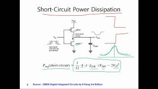
Power Consumption: Refers to the total energy used by a circuit as it operates.
-
Efficiency Metrics: Tools like PDP and EDP used to guide circuit design decisions.
-
Trade-offs: Compromises that designers must consider between aspects like power, performance, and cost.
Examples & Applications
A CMOS circuit operating at 1V has significant leakage at nodes smaller than 45nm, making FinFET a better choice in these scenarios.
FinFETs have shown up to 30-40% power savings at the same performance level compared to CMOS, particularly useful in high-performance computing.
Memory Aids
Interactive tools to help you remember key concepts
Rhymes
CMOS is easy, but leakage is high, / FinFET’s the answer, cost maybe why!
Stories
Imagine two engineers, one working with CMOS who is frustrated by leakage, while another finds success with FinFET, although he pays a premium at the fabrication shop.
Memory Tools
Remember 'LEAD': Leakage in CMOS, Efficiency in FinFET, Area trade-offs, Design optimization.
Acronyms
PDP = Power, Delay and Performance
measure of efficiency to keep your designs in alignment.
Flash Cards
Glossary
- CMOS
Complementary Metal-Oxide-Semiconductor, a technology used for constructing integrated circuits.
- FinFET
A type of non-planar transistor used in advanced semiconductor design for better electrostatics.
- Static Power
Power consumed when a device is idle, significant in submicron technologies.
- Dynamic Power
Power consumption that results from the switching activity of transistors in a circuit.
- PDP
Power-Delay Product, a metric used to evaluate trade-offs between power usage and speed.
- EDP
Energy-Delay Product, a metric that helps optimize performance per watt in circuit design.
Reference links
Supplementary resources to enhance your learning experience.