
Conclusion
Enroll to start learning
You’ve not yet enrolled in this course. Please enroll for free to listen to audio lessons, classroom podcasts and take practice test.
Interactive Audio Lesson
Listen to a student-teacher conversation explaining the topic in a relatable way.
Overview of Power Dissipation
🔒 Unlock Audio Lesson
Sign up and enroll to listen to this audio lesson

Today, we're looking at power dissipation in CMOS circuits. Can anyone tell me the three main components of power consumption?

Is it dynamic, static, and short-circuit power?
Excellent! Dynamic power occurs due to switching activity, while static power arises from leakage currents. Can anyone explain what governs dynamic power?

It depends on the switching activity factor, load capacitance, supply voltage, and frequency.
Correct! A handy acronym to remember this is 'CAVF'—Capacitance, Activity, Voltage, Frequency. Now, can someone share how leakage power impacts design?

It increases as we shrink the transistor sizes, especially under 45nm nodes.
Right! As we move towards smaller nodes, leakage becomes significant. Remember, power dissipation is a critical factor in designing efficient circuits.
Low-Power Techniques
🔒 Unlock Audio Lesson
Sign up and enroll to listen to this audio lesson

Now let's discuss low-power techniques in CMOS design. What strategies do you know?

I know voltage scaling is used to lower dynamic power.
That's right! Voltage scaling is a key approach. Who can tell me about clock gating?
Clock gating disables the clock signal in parts of the circuit that aren't active.
Exactly! This effectively reduces unnecessary power usage. Remember the acronym 'VCD' for Voltage, Clock, and Dynamic power management. Why do we consider multi-Vt cells?
They help balance speed and leakage by using different threshold voltages.
Perfect! It's important to use these techniques wisely to optimize power without sacrificing performance.
Transition to FinFETs
🔒 Unlock Audio Lesson
Sign up and enroll to listen to this audio lesson
Let's move on to FinFETs. Why do you think FinFET technology is necessary at nodes smaller than 22nm?
Because planar CMOS starts to become inefficient due to high leakage?
Exactly! FinFETs offer better gate control over the channel and reduce leakage. How does the structure of FinFETs contribute to their efficiency?
The gate wraps around the fin, providing multiple fins for better drive strength.
Correct! This design allows for stronger control and better performance. What was the power savings from our design example comparing CMOS and FinFET?
The FinFET consumed almost half the dynamic power and significantly less leakage power!
Well summarized! The benefits of FinFET technology play a crucial role in modern VLSI systems.
Introduction & Overview
Read summaries of the section's main ideas at different levels of detail.
Quick Overview
Standard
In this conclusion, we summarize the critical aspects of power dissipation, low-power techniques in CMOS, and the advantages of transitioning to FinFET technology, demonstrating their role in contemporary VLSI systems and the necessity of low-power design.
Detailed
Conclusion
This chapter introduced key concepts in low-power circuit design using CMOS (Complementary Metal-Oxide-Semiconductor) and FinFET (Fin Field-Effect Transistor) technologies. As integrated circuits become more prevalent in battery-powered devices, minimizing power consumption has emerged as a crucial objective for designers. We analyzed:
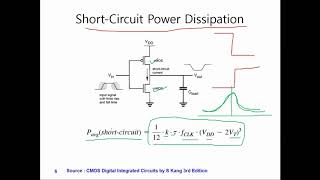
- Sources of Power Dissipation: Addressing the three main components of power consumption in CMOS circuits—dynamic power, static power, and short-circuit power.
- Techniques to Reduce Power in CMOS: Outlining strategies such as voltage scaling, clock gating, and using multi-Vt cells, which aim to conserve energy while maintaining performance.
- Advantages of FinFET Technology: Highlighting how FinFETs effectively manage power dissipation at sub-22nm nodes, thus improving performance and energy efficiency.
- Comparative Design Example: An example showing the power savings achieved when transitioning from CMOS to FinFET technologies.
Low-power design now stands as an essential characteristic of modern VLSI systems, cementing the transition towards FinFETs as a significant advancement for sustaining Moore’s Law in a power-constrained landscape.
Youtube Videos

Audio Book
Dive deep into the subject with an immersive audiobook experience.
Overview of Low-Power Circuit Design
Chapter 1 of 3
🔒 Unlock Audio Chapter
Sign up and enroll to access the full audio experience
Chapter Content
This chapter introduced low-power circuit design using CMOS and FinFET technologies. We analyzed:
Detailed Explanation
The chapter provided a comprehensive introduction to low-power circuit design methodologies, specifically focusing on two technologies: CMOS and FinFET. It highlighted the importance of these technologies in achieving energy efficiency in circuits, especially for modern devices that rely on batteries. The subsequent analysis showcased various aspects of power dissipation, power reduction techniques, and the advantages of moving to FinFETs.
Examples & Analogies
Think of low-power circuit design like designing energy-efficient cars. Just as designers aim to create cars that use less fuel and produce fewer emissions, engineers focus on minimizing power consumption in electronic circuits to prolong battery life and reduce heat output.
Key Sources of Power Dissipation
Chapter 2 of 3
🔒 Unlock Audio Chapter
Sign up and enroll to access the full audio experience
Chapter Content
● Key sources of power dissipation.
● Techniques to reduce power in CMOS.
● Advantages of FinFETs at nanometer-scale nodes.
● A comparative design example that quantifies power savings.
Detailed Explanation
The chapter discusses the fundamental sources of power dissipation in circuits, which include dynamic, static, and short-circuit power. Understanding these sources is essential for creating effective strategies to combat power losses. Additionally, it outlines proven techniques such as voltage scaling and clock gating for reducing power consumption, and finally addresses how FinFETs resolve many challenges presented by conventional CMOS in making circuits operate efficiently at sub-22nm process nodes.
Examples & Analogies
Imagine managing energy use in a household. Just as families learn to reduce their electricity bills by turning off unused lights (comparable to using techniques like clock gating) and utilizing energy-efficient appliances (similar to employing FinFET structures), circuit designers apply similar strategies in design to achieve efficiency.
The Shift Towards FinFETs
Chapter 3 of 3
🔒 Unlock Audio Chapter
Sign up and enroll to access the full audio experience
Chapter Content
Low-power design is now essential, not optional, for modern VLSI systems. The shift toward FinFETs is one of the most impactful changes to sustain Moore’s Law in a power-constrained world.
Detailed Explanation
The shift towards FinFET technology signifies a crucial advancement in semiconductor design. As transistor sizes shrink to maintain Moore’s Law, traditional CMOS faces limitations in managing power leakage and inefficient performance. FinFETs represent a solution that allows for greater energy efficiency and performance at tiny scales, making low-power design mandatory for contemporary chip design. This is increasingly vital as the number of transistors on chips continues to grow while trying to keep power consumption in check.
Examples & Analogies
Just like how manufacturers switched from gas cars to electric cars to meet modern transportation needs, the semiconductor industry is transitioning to FinFETs to ensure that chips are powerful yet efficient as technology advances and demand for portable devices increases.
Key Concepts
-
Power Dissipation: The total power consumed by an integrated circuit, including dynamic and static components.
-
Low-Power Techniques: Strategies aimed at minimizing power consumption in IC design.
-
FinFET Advantages: Improved electrostatic control and reduced leakage power in advanced nodes.
Examples & Applications
A comparison of power profiles shows that a FinFET inverter at 22nm consumes significantly less power than a traditional CMOS inverter.
Implementing clock gating in a complex circuit leads to reduced energy usage by turning off the clock signal in inactive components.
Memory Aids
Interactive tools to help you remember key concepts
Rhymes
In circuits that are CMOS, power can't be lost; with FinFET must be careful, it's a different cost.
Stories
Imagine a race between two devices: CMOS and FinFET. CMOS often runs out of battery -- it's hard to keep pace. But FinFET, being agile, dances through power waste, saving energy and time, winning the low-power race!
Memory Tools
PCD for Power Consumption: P for Power Dissipation, C for Clock Gating, and D for Dynamic Voltage.
Acronyms
SPL for Static Power Leakage
for Subthreshold leakage
for Power Gating
and L for Low-power techniques.
Flash Cards
Glossary
- CMOS
Complementary Metal-Oxide-Semiconductor, a technology for constructing integrated circuits.
- FinFET
Fin Field-Effect Transistor, a type of transistor used for scaling down semiconductor devices.
- Dynamic Power
Power consumed during the switching of transistors.
- Static Power
Power consumed due to leakage current when the transistor is not switching.
- Leakage Power
Power lost due to non-ideal characteristics of transistors, primarily leakage current.
- Power Gating
A technique where transistors are used to disconnect power from inactive circuit components to save energy.
- Voltage Scaling
Reducing the supply voltage to achieve lower power consumption.
- Clock Gating
Disabling the clock signal to inactive portions of circuitry to save energy.
Reference links
Supplementary resources to enhance your learning experience.