
Step 3: Transition to FinFETs
Enroll to start learning
You’ve not yet enrolled in this course. Please enroll for free to listen to audio lessons, classroom podcasts and take practice test.
Interactive Audio Lesson
Listen to a student-teacher conversation explaining the topic in a relatable way.
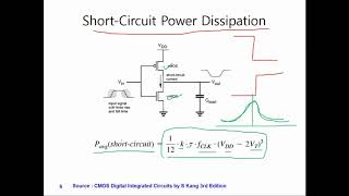
Inefficiency of Planar CMOS
🔒 Unlock Audio Lesson
Sign up and enroll to listen to this audio lesson

Today, we're going to discuss why conventional CMOS technology struggles as we move below 22 nanometers. Can anyone tell me the main issues CMOs faces at smaller nodes?

I think it has to do with leakage currents, right?
Exactly! High leakage is a major problem as transistors shrink. Because the distances are so small, leakage becomes a significant source of power dissipation.

Does that mean they can't control the current effectively anymore?
Yes! Poor electrostatic control leads to unreliable switching. As a result, we need to consider alternatives, such as FinFET technology.

What happens to the performance of devices if we stick with CMOS?
That's a good question! If we continue with CMOS, power consumption would increase dramatically, leading to shorter battery life and overheating issues.

So switching to FinFET is actually a solution to these problems?
Yes, switching to FinFET resolves many issues we face with CMOS at smaller nodes!
In summary, the inefficiency of planar CMOS at nodes smaller than 22nm is a catalyst for transitioning to FinFETs, particularly due to issues surrounding leakage and electrostatic control.
Advantages of FinFET Technology
🔒 Unlock Audio Lesson
Sign up and enroll to listen to this audio lesson

Now let’s delve into the advantages of FinFET technology. Who can name one benefit of using FinFETs?
Reduced leakage?
Correct! With better gate control, FinFETs significantly reduce leakage currents. This is crucial in low-power applications.
What about performance? Do they perform better too?
Absolutely! FinFETs have multiple fins that enhance drive strength, resulting in better performance, especially when switching.
How does the structure of FinFETs help with their performance?
Great question! The gate wraps around the fin on three sides, providing exceptional control over the channel, which directly translates to improved switching behavior.
So it sounds like FinFETs are an essential part of the future of low-power circuit design.
Indeed! In summary, FinFET technology leads to reduced leakage currents, improved drive strength, and better switching performance as compared to traditional CMOS.
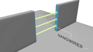
Structural Features of FinFETs
🔒 Unlock Audio Lesson
Sign up and enroll to listen to this audio lesson
Let’s take a closer look at the structure of FinFETs. What distinguishes them from standard transistors?
Is it the fin itself?
Exactly! FinFETs feature a raised fin that acts as the channel. This unique design enhances gate control and lowers leakage.
How does wrapping the gate around the fin work?
Great question! By wrapping the gate around the fin on three sides, we maximize control over the channel, allowing for more efficient switching.
What advantages does this structural design offer in practical applications?
This allows for smaller devices with better performance, leading to advanced low-power applications while maintaining effectiveness in design.
So the structure really makes a difference in how they operate?
That's right! In summary, the unique structure of FinFETs enhances gate control, reduces leakage, and improves overall performance compared to traditional CMOS.
Introduction & Overview
Read summaries of the section's main ideas at different levels of detail.
Quick Overview
Standard
As transistor sizes shrink below 22nm, traditional planar CMOS technology becomes less effective due to high leakage currents and reduced electrostatic control. FinFETs offer significant benefits, including decreased leakage, increased drive strength, and improved switching behavior due to their unique structure. The discussion establishes why FinFETs are crucial in modern low-power circuit design.
Detailed
Detailed Summary
In Section 1.5, we focus on the transition from CMOS technology to FinFETs (Fin Field-Effect Transistors), a change motivated by the limitations of traditional CMOS as technology nodes shrink below 22nm.
Key Points:
- Inefficiency of Planar CMOS: As transistor dimensions decrease, planar CMOS faces challenges such as increasing leakage currents and inability to effectively control the electrostatic behavior of transistors.
- Advantages of FinFET Technology:
- Reduced Leakage: FinFETs provide better gate control over the channel, significantly minimizing leakage currents.
- Increased Drive Strength: The design of FinFETs, which utilizes multiple fins, enables them to deliver higher current while maintaining efficiency.
- Lower Subthreshold Slope: This results in improved switching capabilities, allowing for faster transitions with lower power consumption compared to traditional CMOS.
- Structure of FinFET: The FinFET transistor has a distinctive raised fin of silicon, forming the channel. The gate wraps around this fin on three sides, enhancing control and reducing the short-channel effects that plague smaller CMOS devices.
Overall, the transition to FinFET technology represents a pivotal shift in low-power circuit design, facilitating advancements in integrated circuit performance while adhering to energy efficiency needs.
Youtube Videos

Audio Book
Dive deep into the subject with an immersive audiobook experience.
Introduction to FinFETs
Chapter 1 of 3
🔒 Unlock Audio Chapter
Sign up and enroll to access the full audio experience
Chapter Content
At nodes smaller than 22nm, planar CMOS becomes inefficient due to high leakage and poor electrostatic control. FinFETs offer:
Detailed Explanation
The transition to FinFET technology comes as a solution to certain inefficiencies inherent in traditional planar CMOS circuits, especially as technology nodes shrink below 22 nanometers. As these nodes become smaller, they encounter issues such as increased leakage current and decreased control over the channel due to poor electrostatic control. FinFETs, with their unique structure, provide improvements in these areas.
Examples & Analogies
Think of FinFETs like a multi-level parking garage versus a flat parking lot. In a flat lot, you might find it hard to fit cars in efficiently due to space constraints (analogous to leakage issues in CMOS). A multi-level garage, however, uses space more efficiently by stacking cars, just as FinFETs utilize their three-dimensional structure to better control electrical flow.
Advantages of FinFETs
Chapter 2 of 3
🔒 Unlock Audio Chapter
Sign up and enroll to access the full audio experience
Chapter Content
● Reduced leakage via better gate control over the channel.
● Multiple fins for increased drive strength.
● Lower subthreshold slope, improving switching behavior.
Detailed Explanation
FinFETs have several advantages over traditional CMOS technology. One of the main benefits is reduced leakage current owing to better gate control over the transistor channel. Unlike conventional transistors that may struggle with leakage as they shrink, FinFETs can manage this more effectively. Additionally, the use of multiple fins increases the drive strength, which is crucial for performance. A lower subthreshold slope means that FinFETs can switch states more efficiently, enhancing their overall switching behavior, resulting in less energy wasted and improved power efficiency.
Examples & Analogies
Consider FinFETs as a water faucet where you can precisely control the water flow. A traditional faucet might leak due to a worn-out seal (analogous to leakage in CMOS), leading to wasted water. But with a new, precision tap (the FinFET), you can control and minimize the water escaping (leakage), ensuring just the right amount flows to where it’s needed efficiently.
FinFET Structure
Chapter 3 of 3
🔒 Unlock Audio Chapter
Sign up and enroll to access the full audio experience
Chapter Content
The FinFET structure features a raised fin of silicon that forms the channel. The gate wraps around the fin on three sides, enhancing control.
Detailed Explanation
The design of FinFETs is one of their distinctive features. A raised fin, made of silicon, acts as the channel through which current flows. The gate of the FinFET is wrapped around this fin on three sides, significantly improving the control over the current flowing through the channel. This structure allows for more effective manipulation of the electric field, leading to better performance in terms of switching and lower leakage currents compared to traditional transistor designs.
Examples & Analogies
Imagine wrapping a rubber band around a pencil. If you wrap it tightly around, you can control the pencil's movements more precisely. This is similar to how the gate wraps around the fin in FinFETs, allowing for better control over the channel where the current flows. The more grip you have on the pencil (or in this case, the current), the better you can manage its actions.
Key Concepts
-
Transition to FinFETs: Refers to the shift from traditional CMOS technology to FinFETs to tackle leakage and performance issues.
-
Leakage Reduction: FinFETs offer superior performance in reducing unwanted current flow, critical for low-power design.
-
Gate Control: The unique 3D structure of FinFETs provides enhanced control over the channel compared to planar devices.
Examples & Applications
A CMOS inverter operating at 1.0V with a dynamic power of 1.0µW, compared to a FinFET inverter operating at 0.8V with only 0.51µW of dynamic power.
In practical applications, using FinFETs leads to significant power savings and improved performance metrics for portable devices.
Memory Aids
Interactive tools to help you remember key concepts
Rhymes
In the world of chips where size declines, FinFETs shine while CMOS whines!
Stories
Imagine a giant guarding a treasure, the treasure being power efficiency. The giant represents FinFETs with their multi-fins, expertly controlling the force of leakage that can steal away valuable power.
Memory Tools
FINS - For Improved Nanoscale Switching: a reminder that FinFETs enhance switching efficiency at nanoscale dimensions.
Acronyms
LEAP - Lower Leakage, Enhanced Activity Performance
what FinFETs provide compared to CMOS.
Flash Cards
Glossary
- FinFET
Fin Field-Effect Transistor; a type of transistor characterized by a three-dimensional structure that enables better electrostatic control and reduced leakage.
- Leakage Current
An unwanted flow of current through a transistor when it is in the off state, which increases significantly as transistor sizes decrease.
- Subthreshold Slope
A measure of how effectively a transistor can control the current flow as the gate voltage is varied, with lower values indicating better performance.
- Drive Strength
The ability of a transistor to deliver current and switch states effectively, impacting the speed and performance of the circuit.
- Electrostatic Control
The capability of a transistor gate to influence the current flowing through the channel, crucial for effective switching in reduced-size transistors.
Reference links
Supplementary resources to enhance your learning experience.