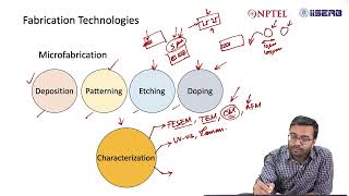
Key Steps in Microfabrication
Interactive Audio Lesson
Listen to a student-teacher conversation explaining the topic in a relatable way.
Lithography
🔒 Unlock Audio Lesson
Sign up and enroll to listen to this audio lesson

Today we're going to focus on lithography. Can anyone tell me what lithography is?

It's a process to transfer patterns onto a substrate.

That's right! Lithography uses a photomask to create designs on the substrate. Now, what are some types of lithography methods?

There’s optical lithography and electron-beam lithography.

Correct! Optical lithography uses UV light while electron-beam lithography offers higher resolution. Remember, resolution can be calculated with the formula: R = k * (λ/NA). Does anyone know what λ and NA stand for?

λ is the wavelength and NA is numerical aperture.

Excellent! Understanding this formula is crucial for predicting the lithography quality. Let's summarize this: Lithography transfers patterns using photomasks with types being optical and electron-beam lithography, defined by their methods like wavelength and numerical aperture.
Etching
🔒 Unlock Audio Lesson
Sign up and enroll to listen to this audio lesson

Now, let’s talk about etching. Why do you think etching is important after lithography?

It helps remove material to create the patterns that were lithographed.

Exactly! Etching can be classified into wet and dry etching. Can someone explain what wet etching is?

Wet etching uses liquid chemicals to remove material.

Good. And dry etching?

Dry etching involves plasma-based techniques like reactive ion etching.

Correct! Dry etching is preferred for high precision in microfabrication. So, let's summarize: Etching is vital for pattern formation, with wet etching using liquid chemicals and dry etching using plasma.
Deposition
🔒 Unlock Audio Lesson
Sign up and enroll to listen to this audio lesson

Finally, let’s discuss deposition. What do we achieve through deposition in microfabrication?

We're adding layers of materials like conductors and insulators.

That's right! We can use methods like Physical Vapor Deposition and Chemical Vapor Deposition. Who can elaborate on PVD?

PVD includes techniques like sputtering and evaporation.

Exactly! And what about CVD?

CVD provides better step coverage.

Perfect! In summary, deposition adds layers of materials essential for building electronic components, using different methods such as PVD and CVD.
Introduction & Overview
Read summaries of the section's main ideas at different levels of detail.
Quick Overview
Standard
The section outlines the critical processes in microfabrication, specifically lithography, etching, and deposition. Each process is essential for producing microstructures on semiconductor materials, enabling advancements in integrated circuits and MEMS technologies.
Detailed
Key Steps in Microfabrication
Microfabrication is a fundamental process in creating miniature devices, primarily on semiconductor materials. This section focuses on three pivotal steps in microfabrication:
1. Lithography
Lithography is the technique that transfers patterns onto a substrate. It starts with a photomask that dictates the desired design. There are various types of lithography, such as optical lithography, which uses UV light, and electron-beam lithography, known for its high resolution but slower speed. The resolution can be calculated using the formula:
\[ R = k \cdot \frac{\lambda}{NA} \]
Where \( \lambda \) represents wavelength, and \( NA \) is the numerical aperture.
2. Etching
Etching is the process that selectively removes material to develop the desired patterns created by lithography. There are two main types: wet etching, which uses liquid chemicals, and dry etching, which employs plasma to achieve high precision.
3. Deposition
Deposition involves adding thin films of materials, such as conductors and insulators, onto the substrate. The most common methods include Physical Vapor Deposition (PVD) and Chemical Vapor Deposition (CVD), each providing different qualities of thin films.
Understanding these steps is crucial for mastering microfabrication, as they form the foundation for producing devices such as integrated circuits and MEMS.
Youtube Videos


Audio Book
Dive deep into the subject with an immersive audiobook experience.
Lithography
Chapter 1 of 3
🔒 Unlock Audio Chapter
Sign up and enroll to access the full audio experience
Chapter Content
1.2.1 Lithography
- Definition: Transfers a pattern from a photomask to a light-sensitive chemical (photoresist) on the substrate.
- Types:
- Optical Lithography: Uses UV light (e.g., photolithography in IC manufacturing).
- Electron-Beam Lithography: Higher resolution but slower (nanoscale features).
- Formula:
- Resolution \( R = k \cdot \frac{\lambda}{NA} \), where \( \lambda \) = wavelength, \( NA \) = numerical aperture.
Detailed Explanation
Lithography is a crucial step in microfabrication where precise patterns are transferred to a substrate. It starts with a photomask, which is like a blueprint, and a light-sensitive material called photoresist. When UV light shines on the photoresist through the photomask, it either hardens or softens depending on the type used. Optical lithography is common for larger features and uses UV light, while electron-beam lithography is more precise but slower, ideal for tiny nanoscale features. The resolution can be calculated using the formula provided, which involves the wavelength of light and the numerical aperture, indicating how well the lens gathers light.
Examples & Analogies
Think of lithography like creating a detailed stencil for a painting. If you shine light through the stencil onto a canvas (the substrate), the areas where light touches will change (the photoresist), and later you can paint over or etch away the unprotected areas to create your artwork. Just like different techniques (UV or electron beams) can yield different style artworks, different lithography techniques help create various electronic components.
Etching
Chapter 2 of 3
🔒 Unlock Audio Chapter
Sign up and enroll to access the full audio experience
Chapter Content
1.2.2 Etching
- Definition: Removes material selectively to create patterns.
- Types:
- Wet Etching: Uses liquid chemicals (isotropic/anisotropic).
- Dry Etching: Plasma-based (e.g., reactive ion etching for high precision).
Detailed Explanation
Etching is the process that shapes the material after lithography by selectively removing areas of the substrate. It can be done in two ways: wet etching, which uses liquid chemicals to dissolve the materials; and dry etching, which employs plasma and is more precise because it can etch in a controlled manner. Wet etching tends to remove material evenly in all directions (isotropic), while dry etching can target specific areas (anisotropic). This selectiveness allows for the creation of intricate patterns needed in microfabrication.
Examples & Analogies
Imagine etching as sculpting a statue from a block of stone. In wet etching, you pour water and let it erode the whole surface evenly like rain eroding soft rock. In dry etching, you use specific tools to carefully chip away at certain areas of a statue rather than the whole block, allowing you to create fine details that wouldn’t be possible with water alone.
Deposition
Chapter 3 of 3
🔒 Unlock Audio Chapter
Sign up and enroll to access the full audio experience
Chapter Content
1.2.3 Deposition
- Definition: Adds thin material layers (conductors, insulators, semiconductors).
- Methods:
- Physical Vapor Deposition (PVD): Sputtering, evaporation.
- Chemical Vapor Deposition (CVD): Higher step coverage (e.g., LPCVD, PECVD).
Detailed Explanation
Deposition is the process of adding layers of material to the substrate where previous patterns are made. These materials can be conductors like metals, insulators also has to be thin layers to ensure device functionality. There are two main methods: Physical Vapor Deposition (PVD), which involves physically vacating material and depositing it onto the substrate, typically through methods like sputtering or evaporation; and Chemical Vapor Deposition (CVD), which involves chemical reactions to create solid materials from gaseous precursors. CVD provides better coverage for complex shapes compared to PVD.
Examples & Analogies
Think of deposition as applying layers of frosting on a cake. PVD is like adding frosting by pouring or spraying it on the top layer, where it might not stick well in the crevices—leading to uneven coverage. CVD, on the other hand, is like using a piping bag with precise control to fill in the curves and contours of a multi-layered cake, ensuring every part gets frosting without gaps.
Key Concepts
-
Lithography: A key step in microfabrication transferring patterns.
-
Etching: Selective material removal to achieve desired patterns.
-
Deposition: Adding layers of material essential for device creation.
Examples & Applications
In semiconductor manufacturing, lithography is used to create circuit patterns on silicon wafers.
Etching is applied to define complex geometries in MEMS sensors.
Deposition techniques are utilized to apply metal layers for interconnects in integrated circuits.
Memory Aids
Interactive tools to help you remember key concepts
Rhymes
To pattern we litho, in chemicals we etch, layer by layer, deposition's our sketch.
Stories
Imagine a chef preparing a cake: first, they outline the shape with a stencil (lithography), then cut out the pieces (etching), and finally, they layer icing and decorations (deposition) to finish the masterpiece.
Memory Tools
LED: Lithography, Etching, Deposition – remember the steps of microfabrication.
Acronyms
LED
Laser Engraving Delivers – a fun way to recall lithography
etching
and deposition.
Flash Cards
Glossary
- Lithography
A process that transfers patterns from a photomask to a light-sensitive chemical on a substrate.
- Etching
A technique that removes material selectively from a substrate to create desired patterns.
- Deposition
The process of adding layers of material onto a substrate to build up structures.
- Optical Lithography
Lithography method that uses UV light for pattern transfer.
- ElectronBeam Lithography
A high-resolution lithography technique that uses electron beams to create patterns.
- Wet Etching
Etching process that uses liquid chemicals to remove material.
- Dry Etching
Etching process utilizing plasma technology for high precision.
- Physical Vapor Deposition (PVD)
A method for depositing thin films using physical processes like sputtering and evaporation.
- Chemical Vapor Deposition (CVD)
A process that deposits thin layers through chemical reactions of gaseous precursors.
Reference links
Supplementary resources to enhance your learning experience.
