Understand the Basic Principles of Microfabrication
Interactive Audio Lesson
Listen to a student-teacher conversation explaining the topic in a relatable way.
Introduction to Microfabrication
🔒 Unlock Audio Lesson
Sign up and enroll to listen to this audio lesson

Today we're diving into microfabrication, which is basically creating tiny structures on materials. Can anyone tell me what materials are generally used in microfabrication?

Isn't silicon one of the main ones used?

Yes, exactly! Silicon is widely used due to its excellent electrical properties. Let's remember that with the mnemonic: **SILICON Stands for Superior In Logic Integrated Circuits On Nodes.** Anyone know the size range of structures created through microfabrication?

I think they are in the micrometer to nanometer scale?

Correct! Great job. Now, what would be some applications of microfabrication?

Integrated circuits and sensors, right?

Absolutely! ICs, MEMS, and even optoelectronics like LEDs. This sets the stage well, as microfabrication underpins many modern technologies.
Steps in Microfabrication: Lithography
🔒 Unlock Audio Lesson
Sign up and enroll to listen to this audio lesson

Now, let's focus on lithography. What does lithography do in microfabrication?

It transfers patterns onto a substrate, right?

Exactly! There are different types of lithography too, like optical lithography and electron-beam lithography. Who can tell me a difference between them?

Optical lithography uses UV light, and it's faster, while electron-beam lithography is slower but can create smaller features?

Spot on! We can remember that with the acronym **E.B. for Electron Beam: Enhanced Detail but Slower.** Now, does anyone know what improves the resolution in lithography?

It's the numerical aperture and the wavelength of light, right?

Exactly! The formula is R = k * λ/NA, where R is resolution. Great job!
Steps in Microfabrication: Etching and Deposition
🔒 Unlock Audio Lesson
Sign up and enroll to listen to this audio lesson

Let's look at etching. What is etching used for in microfabrication?

It removes material to create patterns!

Right! There are wet etching and dry etching. Who remembers the difference?

Wet etching uses liquids and can be isotropic, while dry etching uses plasma and is more precise?

Excellent! And now, what's the purpose of deposition in microfabrication?

Deposition adds thin layers of materials onto a surface!

Great! We have Physical Vapor Deposition (PVD) and Chemical Vapor Deposition (CVD). To remember these, think of **PVD: Particles and Vapor Dance, CVD: Chemicals Vaporize and Deposit.**
Challenges in Microfabrication
🔒 Unlock Audio Lesson
Sign up and enroll to listen to this audio lesson

Now, what challenges do we face in microfabrication?

I think scaling is a big one, especially with Moore's Law!

You're right! Moore's Law addresses the doubling of transistor density. As we shrink features, the limits become a critical issue. Can anyone think of another challenge?

Cost is a challenge too, right? The fabrication plants are really expensive.

Exactly right! These complex systems require immense capital investment. Remember this with the phrase: **Costly Cranes Constructing Complex Circuits!**
Applications of Microfabrication
🔒 Unlock Audio Lesson
Sign up and enroll to listen to this audio lesson

Finally, let's revisit applications. What are some examples of where microfabrication is utilized?

Integrated circuits and sensors like accelerometers.

Yes! And also optoelectronics, such as LEDs and laser diodes. This reinforces how pervasive microfabrication is in tech today!

I can see how it underpins so much of modern technology.

Exactly! Remember, microfabrication is not just about making things small; it's about enhancing innovation across numerous tech spaces.
Introduction & Overview
Read summaries of the section's main ideas at different levels of detail.
Quick Overview
Standard
This section delves into microfabrication, exploring its definition, key steps such as lithography, etching, and deposition, and applications in integrated circuits and sensors, while also addressing challenges like scalability and costs.
Detailed
Understand the Basic Principles of Microfabrication
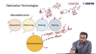
Microfabrication is a process designed to create miniature structures, typically ranging from micrometer to nanometer scales, on semiconductor materials like silicon. It employs a variety of techniques, primarily focusing on lithography, etching, and deposition. The ability to produce integrated circuits (ICs), MEMS, and sensors showcases the critical nature of this field. Importantly, microfabrication blends both top-down approaches, which involve etching bulk materials, and bottom-up methods, which encompass the assembly of atoms to create complex structures. This section further examines key steps in microfabrication, including:
- Lithography: This step is vital for transferring intricate patterns from photomasks onto a light-sensitive layer on the substrate.
- Optical lithography and Electron-Beam lithography are explored, highlighting their respective functionalities and uses.
- Etching: It involves selective material removal to create distinct patterns, distinguishing between wet and dry etching techniques.
- Deposition: This process adds various materials, such as conductors or insulators, onto substrates using methods like PVD and CVD.
Silicon is established as the primary semiconductor material due to its superior electrical characteristics, while several compound semiconductors are also discussed for specialized applications. Given the need for high precision in microfabrication, cleanroom protocols play a significant role in maintaining defect-free environments. The chapter concludes by addressing the major challenges in the field, such as the limits of Moore’s Law at nanoscale dimensions and the substantial costs associated with fabrication facilities. Understanding these principles is essential for engaging with future technologies that rely on microfabrication.
Youtube Videos


Audio Book
Dive deep into the subject with an immersive audiobook experience.
Introduction to Microfabrication
Chapter 1 of 4
🔒 Unlock Audio Chapter
Sign up and enroll to access the full audio experience
Chapter Content
1.1 Introduction to Microfabrication
- Definition:
- Microfabrication is the process of creating miniature structures (micrometer to nanometer scale) on semiconductor materials (e.g., silicon) using techniques like lithography, etching, and deposition.
- Key Concepts:
- Enables production of integrated circuits (ICs), MEMS, and sensors.
- Combines top-down (etching bulk material) and bottom-up (atomic assembly) approaches.
Detailed Explanation
Microfabrication refers to techniques used to create tiny structures that can be measured in micrometers or nanometers. This process is essential for manufacturing components like integrated circuits (ICs) which are used in computers, as well as micro-electromechanical systems (MEMS) that are found in various sensors. In microfabrication, two main strategies are employed: top-down approaches, which involve etching away from larger pieces of material, and bottom-up approaches, which build structures atom by atom.
Examples & Analogies
Think of microfabrication like sculpting a tiny statue. In a top-down approach, you might start with a large block of stone and chisel away material to form the statue – this is similar to etching. In a bottom-up approach, it’s like stacking tiny bricks to build the statue, where you carefully place each brick in the right position to create the overall shape.
Key Steps in Microfabrication
Chapter 2 of 4
🔒 Unlock Audio Chapter
Sign up and enroll to access the full audio experience
Chapter Content
1.2 Key Steps in Microfabrication
1.2.1 Lithography
- Definition: Transfers a pattern from a photomask to a light-sensitive chemical (photoresist) on the substrate.
- Types:
- Optical Lithography: Uses UV light (e.g., photolithography in IC manufacturing).
- Electron-Beam Lithography: Higher resolution but slower (nanoscale features).
- Formula:
- Resolution \( R = k \cdot \frac{\lambda}{NA} \), where \( \lambda \) = wavelength, \( NA \) = numerical aperture.
Detailed Explanation
Lithography is a critical step in microfabrication, where specific patterns are created on a substrate using light-sensitive materials called photoresists. This process can be achieved through various techniques, with Optical Lithography being the most common, using ultraviolet light to transfer patterns. Electron-Beam Lithography provides highly detailed patterns but at a slower pace. The resolution of these lithographic methods can be quantified using a formula that takes into account factors like the wavelength of light used.
Examples & Analogies
Imagine printing a photo on paper. The lithographic process is like creating a stencil of that photo. You place the stencil over the photo-paper and expose it to light; wherever the stencil blocks the light, the paper remains untouched. Using these principles, intricate electronic components can be printed directly onto semiconductor wafers.
Etching
Chapter 3 of 4
🔒 Unlock Audio Chapter
Sign up and enroll to access the full audio experience
Chapter Content
1.2.2 Etching
- Definition: Removes material selectively to create patterns.
- Types:
- Wet Etching: Uses liquid chemicals (isotropic/anisotropic).
- Dry Etching: Plasma-based (e.g., reactive ion etching for high precision).
Detailed Explanation
Etching is a technique used to selectively remove material from a substrate to form desired patterns. This process can be accomplished in two main ways: Wet Etching, which uses liquid chemicals, and Dry Etching, which utilizes plasma or gas to etch away material at a finer precision. Wet Etching can be isotropic, where the etching proceeds uniformly in all directions, or anisotropic, where it is directional, focusing on specific areas.
Examples & Analogies
Consider etching like carving a design on a soft surface like butter. If you use a hot knife (dry etching), you can create very precise, clean lines, similar to how dry etching works with gases. In contrast, using a spoon (wet etching) might cause the butter to spread more and lose definition in the design's edges, akin to the isotropic effect of wet etching.
Deposition
Chapter 4 of 4
🔒 Unlock Audio Chapter
Sign up and enroll to access the full audio experience
Chapter Content
1.2.3 Deposition
- Definition: Adds thin material layers (conductors, insulators, semiconductors).
- Methods:
- Physical Vapor Deposition (PVD): Sputtering, evaporation.
- Chemical Vapor Deposition (CVD): Higher step coverage (e.g., LPCVD, PECVD).
Detailed Explanation
Deposition is a process of adding thin layers of material onto a substrate. This is crucial in creating the different layers in microelectronic devices, such as conductive or insulating layers. Two key methods of deposition are Physical Vapor Deposition (PVD), which involves physical processes like sputtering or evaporation to lay down materials, and Chemical Vapor Deposition (CVD), which involves chemical reactions to form distinct layers with better coverage over complex surfaces.
Examples & Analogies
Think of deposition as icing a cake. When you place icing on a cake, you spread it evenly to create a thin layer. Similarly, during deposition, materials are applied in very fine layers to achieve the desired thickness and properties required for the final electronic device.
Key Concepts
-
Microfabrication: Process of creating miniature structures on semiconductor materials.
-
Lithography: Technique for transferring patterns onto substrates using a photomask.
-
Etching: A process to selectively remove materials to create defined geometries.
-
Deposition: Methods to add layers of materials onto surfaces.
-
Silicon: Dominates the semiconductor industry for its excellent electrical properties.
-
Cleanroom: Controlled environment critical for microfabrication processes.
Examples & Applications
The manufacturing of microprocessors, where millions of transistors are created on a silicon wafer.
The production of MEMS accelerometers used in smartphones and automotive applications.
Memory Aids
Interactive tools to help you remember key concepts
Rhymes
To make things small with details galore, microfabrication opens technology's door.
Stories
Once, in a lab, there was a tiny silicon valley where each drop of chemical crafted castles in the atomic scale, shaping the future.
Memory Tools
Remember the steps of microfabrication as L.E.D.: Lithography, Etching, Deposition!
Acronyms
For cleanrooms, remember C.L.E.A.N.
Controlled environment
Limit particles
Ensure safety
Accommodate protocols
Necessary for success.
Flash Cards
Glossary
- Microfabrication
The process of creating miniature structures on semiconductor materials.
- Lithography
A technique for transferring patterns onto substrates.
- Etching
A process that removes material selectively to create desired patterns.
- Deposition
A method to add thin layers of materials onto surfaces.
- Silicon
A semiconductor material widely used in the fabrication of electronic components.
- Cleanroom
A controlled environment with limited airborne particles necessary for defect-free manufacturing.
- Compound Semiconductors
Semiconductors made from multiple elements, allowing for specialized applications.
Reference links
Supplementary resources to enhance your learning experience.
